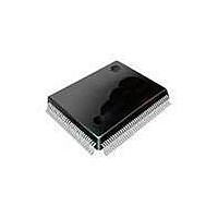
SAA7115HLBE NXP Semiconductors, SAA7115HLBE Datasheet - Page 258

SAA7115HLBE
Manufacturer Part Number
SAA7115HLBE
Description
Video ICs ADV DGTL VIDEO DECODR
Manufacturer
NXP Semiconductors
Datasheet
1.SAA7115HLBE.pdf
(548 pages)
Specifications of SAA7115HLBE
Operating Supply Voltage
3.3 V
Maximum Operating Temperature
+ 70 C
Package / Case
SOT-407
Minimum Operating Temperature
0 C
Mounting Style
SMD/SMT
Number Of Channels
2
Resolution
8 bit
Lead Free Status / RoHS Status
Lead free / RoHS Compliant
Other names
SAA7115HL/V1,557 SAF7115HLBE
- Current page: 258 of 548
- Download datasheet (6Mb)
PNX1300/01/02/11 Data Book
A detailed description of the configuration of the receiver
can be found in the SSI_CTL and SSI_CSR register de-
scription
SSI_RxDR is a 32-bit MMIO receive data register.
Due to the possibility of speculative reading of the
SSI_RxDR, the read itself can not be implemented to ac-
knowledge the data as a side effect. For this reason an
explicit acknowledge mechanism is provided by the
SSI_RxACK register.
The SSI_RxACK is a 1-bit MMIO register that is used to
signal the SSI receiver state machine that a word has
been successfully read from the SSI_RxDR.
17-4
Figure 17-4. The Sync Serial Interface Transmit Block Diagram
Figure 17-5. The SSI receive block diagram
SSI_RxDATA
(17.10.1
SSI_TxDATA
SSI_RxCLK
SSI_RxFSX
and 17.10.2)
PRELIMINARY SPECIFICATION
TxCLK
TxFSX
Shift Reg
Shift Reg
Receive
Transmit
RxSR
TxSR
Writing a ‘1’ to this register initiates updating of the inter-
nal state. Writing a ‘0’ has no effect.
The register cannot be read, its effect may be observed
in the WAR field of the SSI_CSR.
The status fields of the SSI_CSR will update within 1
highway clock cycle after writing to the SSI_RXACK reg-
ister.
64-byte Receive Buffer
64-byte Transmit Buffer
Receive Control Logic
Transmit Control Logic
Status Reg
Status Reg
Transmit
Receive
Philips Semiconductors
Control Reg
SSI_RXDR
Control Reg
SSI_TXDR
Data Reg
Data Reg
Receive
Receive
Transmit
Transmit
Related parts for SAA7115HLBE
Image
Part Number
Description
Manufacturer
Datasheet
Request
R
Part Number:
Description:
Ntsc/pal/secam 9-bit Video Decoder
Manufacturer:
NXP Semiconductors
Datasheet:
Part Number:
Description:
NXP Semiconductors designed the LPC2420/2460 microcontroller around a 16-bit/32-bitARM7TDMI-S CPU core with real-time debug interfaces that include both JTAG andembedded trace
Manufacturer:
NXP Semiconductors
Datasheet:

Part Number:
Description:
NXP Semiconductors designed the LPC2458 microcontroller around a 16-bit/32-bitARM7TDMI-S CPU core with real-time debug interfaces that include both JTAG andembedded trace
Manufacturer:
NXP Semiconductors
Datasheet:
Part Number:
Description:
NXP Semiconductors designed the LPC2468 microcontroller around a 16-bit/32-bitARM7TDMI-S CPU core with real-time debug interfaces that include both JTAG andembedded trace
Manufacturer:
NXP Semiconductors
Datasheet:
Part Number:
Description:
NXP Semiconductors designed the LPC2470 microcontroller, powered by theARM7TDMI-S core, to be a highly integrated microcontroller for a wide range ofapplications that require advanced communications and high quality graphic displays
Manufacturer:
NXP Semiconductors
Datasheet:
Part Number:
Description:
NXP Semiconductors designed the LPC2478 microcontroller, powered by theARM7TDMI-S core, to be a highly integrated microcontroller for a wide range ofapplications that require advanced communications and high quality graphic displays
Manufacturer:
NXP Semiconductors
Datasheet:
Part Number:
Description:
The Philips Semiconductors XA (eXtended Architecture) family of 16-bit single-chip microcontrollers is powerful enough to easily handle the requirements of high performance embedded applications, yet inexpensive enough to compete in the market for hi
Manufacturer:
NXP Semiconductors
Datasheet:
Part Number:
Description:
The XA-S3 device is a member of Philips Semiconductors? XA(eXtended Architecture) family of high performance 16-bitsingle-chip microcontrollers
Manufacturer:
NXP Semiconductors
Datasheet:

Part Number:
Description:
The NXP BlueStreak LH75401/LH75411 family consists of two low-cost 16/32-bit System-on-Chip (SoC) devices
Manufacturer:
NXP Semiconductors
Datasheet:

Part Number:
Description:
The NXP LPC3130/3131 combine an 180 MHz ARM926EJ-S CPU core, high-speed USB2
Manufacturer:
NXP Semiconductors
Datasheet:

Part Number:
Description:
The NXP LPC3141 combine a 270 MHz ARM926EJ-S CPU core, High-speed USB 2
Manufacturer:
NXP Semiconductors

Part Number:
Description:
The NXP LPC3143 combine a 270 MHz ARM926EJ-S CPU core, High-speed USB 2
Manufacturer:
NXP Semiconductors

Part Number:
Description:
The NXP LPC3152 combines an 180 MHz ARM926EJ-S CPU core, High-speed USB 2
Manufacturer:
NXP Semiconductors

Part Number:
Description:
The NXP LPC3154 combines an 180 MHz ARM926EJ-S CPU core, High-speed USB 2
Manufacturer:
NXP Semiconductors


