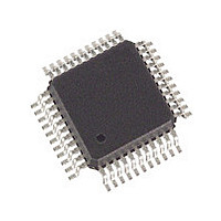
SLXT332QE.G2 Cortina Systems Inc, SLXT332QE.G2 Datasheet - Page 12

SLXT332QE.G2
Manufacturer Part Number
SLXT332QE.G2
Description
Manufacturer
Cortina Systems Inc
Datasheet
1.SLXT332QE.G2.pdf
(45 pages)
Specifications of SLXT332QE.G2
Operating Supply Voltage (typ)
5V
Screening Level
Industrial
Mounting
Surface Mount
Operating Supply Voltage (min)
4.75V
Operating Supply Voltage (max)
5.25V
Operating Temperature (min)
-40C
Operating Temperature (max)
85C
Lead Free Status / RoHS Status
Not Compliant
Available stocks
Company
Part Number
Manufacturer
Quantity
Price
Company:
Part Number:
SLXT332QE.G2
Manufacturer:
ICS
Quantity:
427
LXT332
Datasheet
249075, Revision 2.0
26 June 2007
Table 1
Cortina Systems
1. DI = Digital Input; DO = Digital Output; DI/O = Digital Input/Output; AI = Analog Input; AO = Analog Output; S = Power
QFP
Pin
11
10
12
13
14
15
16
17
18
19
20
21
22
23
26
24
25
27
28
8
9
Supply.
PLCC
Pin
14
17
15
16
18
19
20
21
22
23
24
25
26
27
28
29
32
30
31
33
34
Host Mode and Bipolar Host Mode Pin Descriptions (Sheet 2 of 3)
®
LXT332 Dual T1/E1 Line Interface Unit with Crystal-less Jitter Attenuation
RRING0
RRING1
Symbol
TRING0
TRING1
TGND0
TVCC0
TVCC1
TGND1
JASEL
RTIP0
RTIP1
TTIP0
TTIP1
CLKE
DFM
VCC
PS0
PD0
PD1
PS1
SDI
I/O
AO
AO
DO
DO
DO
AO
AO
DI
AI
AI
DI
AI
AI
DI
DI
DI
S
S
S
S
S
1
Transmit Tip and Ring
drive a 35
give the desired pulse height. See
Ground
+ 5 VDC
than ± 0.3 V.
Driver Failure Monitor. This signal goes High to indicate a driver output short in one or
both ports.
Port Select
each read or write operation, PS0 must transition from High to Low, and remain Low.
Pattern Detect
functions as an Alarm Indication Signal (AIS). The AIS pattern is detected by the
receiver, independent of any loopback mode. PD0 goes High when less than three
zeros have been detected in any string of 2048 bits. PD0 returns Low when the
received signal contains more than three zeros in 2048 bits.
If the QRSS function is enabled by the VCQE pin, PD0 remains High until pattern sync
is reached with the received signal. Once pattern lock is obtained, PD0 goes Low. The
sync/out
errors cause PD0 to go High for half a clock cycle. PD0 can be used to trigger an
external error counter.
Receive Tip and Ring
should be connected to the line through a center
Figure 14
Clock Edge Select. When CLKE is High, RPOS/RNEG or RDATA outputs are valid on
the falling edge of RCLK, and SDO is valid on the rising edge of SCLK.
When CLKE is Low, RPOS/RNEG or RDATA outputs are valid on the rising edge of
RCLK, and SDO is valid on the falling edge of SCLK.
Receive Tip and Ring
should be connected to the line through a center
Figure 14
Pattern Detect
description for details.
Serial Data Input. Write data to the LXT332 registers is input on this pin. SDI is
sampled on the rising edge of SCLK.
Port Select
write operation, PS1 must transition from High to Low, and remain Low.
Transmit Tip and Ring
drive a 35
give the desired pulse height. See
+ 5 VDC
than ± 0.3 V.
Ground
+5 VDC. Power supply for all circuits except the transmit drivers.
Jitter Attenuation Select. When JASEL is High, the Jitter Attenuation (JA) circuits are
placed in the receive paths. When JASEL is Low, the JA circuits are placed in the
transmit paths. When JASEL is clocked with MCLK, the JA circuits are disabled.
-
-
-
-
-
of
through
through
Port 0 Transmit Driver. Ground return for the TVCC0 power supply.
Port 1 Transmit Driver. Ground return for the TVCC1 power supply.
-
Port 0 Transmit Driver. TVCC0 must not vary from TVCC1 or VCC by more
-
Port 1 Transmit Driver. TVCC1 must not vary from TVCC0 or VCC by more
-
200 Ω load. Line matching resistors and transformers can be selected to
sync criteria is: less than 3/4 errors in 128 bits. After sync acquisition, bit
200 Ω load. Line matching resistors and transformers can be selected to
-
-
Port 0. This signal selects the serial interface registers for port 0. For
Port 1. Selects the serial interface registers for port 1. For each read or
-
-
Port 0. Unless the QRSS function is selected by the VCQE pin, PD0
Port 1. Reports AIS and QRSS pattern reception. See PD0 signal
Figure 16
Figure 16
-
-
-
-
Port 0. These pins comprise the receive line interface and
Port 1. These pins comprise the receive line interface and
Port 0. These pins are differential driver outputs designed to
Port 1. These pins are differential driver outputs designed to
for details.
for details.
Table 10
Table 10
Description
and
and
Figure 14
Figure 14
-
-
tapped 1:2 transformer. See
tapped 1:2 transformer. See
3.0 Pin Assignments and Signal
through
through
Figure 16
Figure 16
Descriptions
for details.
for details.
Page 12


