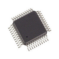
SLXT332QE.G2 Cortina Systems Inc, SLXT332QE.G2 Datasheet - Page 7

SLXT332QE.G2
Manufacturer Part Number
SLXT332QE.G2
Description
Manufacturer
Cortina Systems Inc
Datasheet
1.SLXT332QE.G2.pdf
(45 pages)
Specifications of SLXT332QE.G2
Operating Supply Voltage (typ)
5V
Screening Level
Industrial
Mounting
Surface Mount
Operating Supply Voltage (min)
4.75V
Operating Supply Voltage (max)
5.25V
Operating Temperature (min)
-40C
Operating Temperature (max)
85C
Lead Free Status / RoHS Status
Not Compliant
Available stocks
Company
Part Number
Manufacturer
Quantity
Price
Company:
Part Number:
SLXT332QE.G2
Manufacturer:
ICS
Quantity:
427
LXT332
Datasheet
249075, Revision 2.0
26 June 2007
2.0
2.1
2.1.1
2.1.2
2.1.3
2.1.4
2.1.5
2.2
2.2.1
2.2.2
Cortina Systems
Overview
In addition to the inherent advantages of a dual LIU, the LXT332 also provides several
advanced features that are not available in other LXT300-series devices. All of the added
features are easily implemented. Many require only a clock pulse to change from one
mode to another. Some features are available in Host mode only.
Standard LXT332 Features
Tri
All LXT332 output pins can be forced to tri-state (high-Z). Tri-state is controlled by the
TRSTE pin.
Bipolar or Unipolar Data I/O
The LXT332 to framer interface can be either bipolar (default) or unipolar (selectable).
The unipolar I/O mode is selected by applying MCLK to the TRSTE pin.
B8ZS or HDB3 Zero Suppression
The LXT332 incorporates zero suppression encoders and decoders for use in the unipolar
data I/O mode. The encoders/decoders can be activated or deactivated by changing the
logic level on the re-mapped TNEG pin.
Selectable Jitter Attenuation
Jitter attenuation can be placed in either the transmit or receive path or deactivated. The
Jitter Attenuation Select (JASEL) pin selects the jitter attenuation path. No crystal is
required.
Dual Loopback
Dual Loopback (DLOOP) enables simultaneous loopbacks to both the framer and the line.
The TCLK, TPOS and TNEG framer inputs are routed through the jitter attenuator and
looped back to the RCLK, RPOS and RNEG outputs. The RTIP/RRING line inputs are
looped back through the timing recovery block and line driver onto the TTIP/TRING
outputs.
Additional Host
High Frequency Clocks
The LXT332 provides a pair of high frequency clock outputs, one for each LIU. These
8x clocks (12.352 MHz for T1, 16.384 MHz for E1) are tied to the de-jittered clock from the
JA of the respective LIU.
Bipolar Violation Insertion
The same pins which provide the high frequency clocks can also be used to insert bipolar
violations into the outgoing data stream. Violations can be inserted into each LIU port
independently.
®
LXT332 Dual T1/E1 Line Interface Unit with Crystal-less Jitter Attenuation
-
state Outputs
-
Mode Features
2.0 Overview
Page 7


