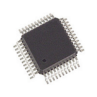
SLXT332QE.G2 Cortina Systems Inc, SLXT332QE.G2 Datasheet - Page 31

SLXT332QE.G2
Manufacturer Part Number
SLXT332QE.G2
Description
Manufacturer
Cortina Systems Inc
Datasheet
1.SLXT332QE.G2.pdf
(45 pages)
Specifications of SLXT332QE.G2
Operating Supply Voltage (typ)
5V
Screening Level
Industrial
Mounting
Surface Mount
Operating Supply Voltage (min)
4.75V
Operating Supply Voltage (max)
5.25V
Operating Temperature (min)
-40C
Operating Temperature (max)
85C
Lead Free Status / RoHS Status
Not Compliant
Available stocks
Company
Part Number
Manufacturer
Quantity
Price
Company:
Part Number:
SLXT332QE.G2
Manufacturer:
ICS
Quantity:
427
LXT332
Datasheet
249075, Revision 2.0
26 June 2007
5.0
5.1
5.2
5.3
5.4
Cortina Systems
Application Information
Power Requirements
The LXT332 is a low-power CMOS device. It operates from a single +5 V power supply
which can be tied to all three VCC pins. However, all inputs must be within ±0.3 V of each
other, and decoupled to their respective grounds separately. Isolation between the
transmit and receive circuits is provided internally. During normal operation or local
loopback, the transmitter powers down if TCLK is not supplied.
Transformers
The transformer specifications listed in
for balanced transmit or receive lines.
transformers to produce a variety of return loss values depending on the LEN code
settings chosen for a specific design.
Line Protection
On the receive side, the 1 kΩ series resistors protect the receiver against current surges
coupled into the device. Due to the high receiver impedance (40 kΩ typical) the resistors
do not affect the receiver sensitivity.
On the transmit side, the Schottky diodes D1-D4 protect the output driver. While not
mandatory for normal operation, these protection elements are strongly recommended to
improve the design’s robustness.
1.544 Mbps T1 Applications
Figure 14
at the top. Host mode is selected by applying clock to SPE. Other mode selection pins are
shown at the bottom. With the TRSTE pin switched Low, the LXT332 operates in the
bipolar I/O mode. Driving JASEL Low switches the jitter attenuation circuits into the
transmit paths for both LIU ports.
Figure 14
(CLAD) converts the 2.048 MHz backplane clock to provide the 1.544 MHz input to the
MCLK and TCLK inputs of both LIU ports.
The DFM and PD indicators and high frequency clocks are grouped at the lower left.
These outputs are available to drive optional external circuits. The transmit driver power
supply pins (TVCC0 and TVCC1) are tied to a common bus with 68 µF decoupling
capacitors installed. The power supply for the remaining (non-driver) circuitry (VCC) uses
1.0 µF and 0.1 µF decoupling capacitors.
The line interface circuitry is identical for both LIU ports. The precision resistors in line with
the transmit transformer provide optimal return loss. The recommended transformer/
resistor combinations are listed in
the receive side.
®
LXT332 Dual T1/E1 Line Interface Unit with Crystal-less Jitter Attenuation
shows a typical T1 Host mode application. The serial interface pins are grouped
shows a pair of framers (a dual framer could also be used). A Clock Adapter
Table
Table 10
Table 9
10. Center tapped 2:1 transformers are used on
provide the correct impedance matching
shows the combinations of resistors and
5.0 Application Information
Page 31


