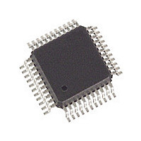
SLXT332QE.G2 Cortina Systems Inc, SLXT332QE.G2 Datasheet - Page 21

SLXT332QE.G2
Manufacturer Part Number
SLXT332QE.G2
Description
Manufacturer
Cortina Systems Inc
Datasheet
1.SLXT332QE.G2.pdf
(45 pages)
Specifications of SLXT332QE.G2
Operating Supply Voltage (typ)
5V
Screening Level
Industrial
Mounting
Surface Mount
Operating Supply Voltage (min)
4.75V
Operating Supply Voltage (max)
5.25V
Operating Temperature (min)
-40C
Operating Temperature (max)
85C
Lead Free Status / RoHS Status
Not Compliant
Available stocks
Company
Part Number
Manufacturer
Quantity
Price
Company:
Part Number:
SLXT332QE.G2
Manufacturer:
ICS
Quantity:
427
LXT332
Datasheet
249075, Revision 2.0
26 June 2007
4.7.1
4.7.2
Table 6
Cortina Systems
The Clock Edge (CLKE) signal determines when the SDO and receive data outputs are
valid, relative to the Serial Clock (SCLK) or RCLK as listed in
Specifications section for SIO timing.
Serial Input Word
Figure 5
in the Address/Command byte, corresponding to address 16. Bit 1 of the serial Address/
Command byte provides Read/Write (R/W) control when the chip is accessed. The R/W
bit is set to logic 1 to read the data output byte from the chip, and set to logic 0 to write the
input data byte to the chip.
The second 8 bits of a write operation, the Data Input byte, clear Loss of Signal (LOS) and
Driver Fail Monitor (DFM) interrupts, reset the chip, and control diagnostic modes. The
first 2 bits (D0 – D1) clear and/or mask LOS and DFM interrupts, and the last 3 bits (D5 -
D7) control operating modes (normal and diagnostic) and chip reset. Refer to
details on bits D5 – D7 of the Serial Input Word.
Serial Output Word
Figure 6
receives an Address/Command byte. If SDI receives a write command (R/W = 0), SDO
remains in high impedance. If the command is a read (R/W = 1), then SDO becomes
active after the last Command/Address bit (A6) and remains active for eight SCLK cycles.
Typically the first bit out of SDO changes the state of SDO from high-z to a Low/High. This
occurs approximately 100 ns after the eighth falling edge of SCLK.
The output data byte reports Loss of Signal (LOS) and Driver Fail Monitor (DFM)
conditions, equalizer settings, and operating modes (normal or diagnostic). The first 5 bits
(D0 - D4) report LOS and DFM status, and the Line Length Equalizer settings. The last
3 bits (D5 - D7) report operating modes and interrupt status.
If the INTx line for port x is High (no interrupt is pending), bits D5 - D7 report the operating
modes listed in
other reports and bits D5 - D7 reflect the interrupt status as listed in
CLKE Settings
®
LXT332 Dual T1/E1 Line Interface Unit with Crystal-less Jitter Attenuation
CLKE
HIGH
LOW
shows the Serial Input data structure. The LXT332 is addressed by setting bit A4
shows the Serial Output data structure. SDO is high impedance when SDI
RPOS/RNEG
RPOS/RNEG
Table
Output
RDATA
RDATA
SDO
SDO
8. If the INTx line for port x is Low, the interrupt status overrides all
RCLK
RCLK
RCLK
RCLK
Clock
SCLK
SCLK
Valid Edge
Falling
Falling
Falling
Rising
Rising
Rising
Table
6. Refer to the Test
Table
4.7 Host Mode Control
6.
Table 7
Page 21
for


