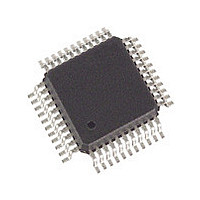
SLXT332QE.G2 Cortina Systems Inc, SLXT332QE.G2 Datasheet - Page 25

SLXT332QE.G2
Manufacturer Part Number
SLXT332QE.G2
Description
Manufacturer
Cortina Systems Inc
Datasheet
1.SLXT332QE.G2.pdf
(45 pages)
Specifications of SLXT332QE.G2
Operating Supply Voltage (typ)
5V
Screening Level
Industrial
Mounting
Surface Mount
Operating Supply Voltage (min)
4.75V
Operating Supply Voltage (max)
5.25V
Operating Temperature (min)
-40C
Operating Temperature (max)
85C
Lead Free Status / RoHS Status
Not Compliant
Available stocks
Company
Part Number
Manufacturer
Quantity
Price
Company:
Part Number:
SLXT332QE.G2
Manufacturer:
ICS
Quantity:
427
LXT332
Datasheet
249075, Revision 2.0
26 June 2007
4.7.3
4.8
4.9
4.9.1
Cortina Systems
Interrupt Handling
The Host mode provides two latched Interrupt output pins, INT0 and INT1, one for each
LIU port. An interrupt is triggered by a change in the LOS or DFM bits (D0 and D1 of the
output data byte, respectively). As shown in
either or both interrupt generators can be masked by writing a one to the respective bit of
the input data byte (D0 = LOS, D1 = DFM). When an interrupt has occurred, the INTx
output pin is pulled Low. The output stage of each INTx pin consists only of a pull-down
device. Hence, an external pull-up resistor is required. The interrupt is cleared as follows:
Hardware Mode Control
Hardware control is the default operating mode. The LXT332 operates in Hardware mode
unless the LEN11/SPE pin is clocked. In Hardware mode the transceiver is controlled
through individual pins; a µP is not required. The SIO pins are re-mapped to provide
control functions. Data I/O mode selection is unaffected by the control mode. The TRSTE
pin selects either unipolar or bipolar data I/O. In Hardware mode the RPOS/RNEG or
RDATA/BPV outputs are valid on the rising edge of RCLK.
Diagnostic Mode Operation
The LXT332 offers multiple diagnostic modes. Local Loopback (LLOOP), Remote
Loopback (RLOOP), Dual Loopback (DLOOP) and Transmit All Ones (TAOS) are
available under both Host and Hardware control. An additional Quasi-Random Signal
Source (QRSS) mode is available under Host control only.
In Host mode, diagnostic modes are selected by writing the appropriate SIO bits. In
Hardware mode, diagnostic modes are selected by a combination of pin settings. The pins
must be held at the specified levels for a minimum of 20 ns. The SIO bit names (Host
mode) and pin identifiers (Hardware mode) for diagnostic functions are identical. Where a
particular function can be enabled in either mode, 1 = High and 0 = Low.
Transmit All Ones
Transmit All Ones (TAOS) is selected when TAOS = 1 and RLOOP = 0. In TAOS mode
the TPOS and TNEG inputs are ignored. The TAOS reference clock is determined by
setting the jitter attenuator. When jitter attenuation is set for the transmit side, MCLK is
used as the TAOS reference clock and TCLK is the fall back clock. When JA is set for the
receive side, TCLK is the TAOS reference clock and MCLK is the fall back clock. When JA
is inactive, MCLK is the TAOS reference clock and TCLK is the fall back. TAOS can be
commanded simultaneously with Local Loopback as shown in
during Remote and Dual Loopback.
®
1. If one or both interrupt bits (LOS or DFM, D0 and D1 of the output data byte) = 1,
2. If neither LOS or DFM = 1, the interrupt will be cleared by resetting the chip. To reset
LXT332 Dual T1/E1 Line Interface Unit with Crystal-less Jitter Attenuation
writing a 1 to the respective input bit (D0 or D1, respectively, of the input data byte)
will clear the interrupt. Leaving a 1 in either of these bit positions will effectively mask
the associated interrupt. To re-enable the interrupt capability, reset D0 and/or D1 to 0.
the chip, set data input bits D5 and D6 = 1, and D7 = 0.
(See
Figure 8
)
Figure 7, Interrupt Handling, on page
Figure
4.8 Hardware Mode Control
9, but is inhibited
24,
Page 25


