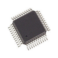
SLXT332QE.G2 Cortina Systems Inc, SLXT332QE.G2 Datasheet - Page 15

SLXT332QE.G2
Manufacturer Part Number
SLXT332QE.G2
Description
Manufacturer
Cortina Systems Inc
Datasheet
1.SLXT332QE.G2.pdf
(45 pages)
Specifications of SLXT332QE.G2
Operating Supply Voltage (typ)
5V
Screening Level
Industrial
Mounting
Surface Mount
Operating Supply Voltage (min)
4.75V
Operating Supply Voltage (max)
5.25V
Operating Temperature (min)
-40C
Operating Temperature (max)
85C
Lead Free Status / RoHS Status
Not Compliant
Available stocks
Company
Part Number
Manufacturer
Quantity
Price
Company:
Part Number:
SLXT332QE.G2
Manufacturer:
ICS
Quantity:
427
LXT332
Datasheet
249075, Revision 2.0
26 June 2007
Table 3
Cortina Systems
1.
2. DI = Digital Input; DO = Digital Output; DI/O = Digital Input/Output; AI = Analog Input; AO = Analog Output; S = Power Supply.
QFP
Pin
11
10
12
13
14
15
16
17
18
19
20
21
22
23
26
24
25
27
28
29
30
31
32
8
9
Table 1
PLCC
describes the pins that do not change function in Unipolar Host mode and functions of pins unique to Bipolar mode.
Pin
14
17
15
16
18
19
20
21
22
23
24
25
26
27
28
29
32
30
31
33
34
35
36
37
38
Hardware Mode and Bipolar Hardware Mode Pin Descriptions
®
LXT332 Dual T1/E1 Line Interface Unit with Crystal-less Jitter Attenuation
RLOOP0
RLOOP1
LLOOP0
LLOOP1
RRING0
RRING1
Symbol
TRING0
TRING1
TGND1
TGND0
TVCC0
TVCC1
TAOS1
JASEL
LEN01
LEN11
LEN21
RTIP0
RTIP1
TTIP0
TTIP1
LOS0
LOS1
DFM
VCC
I/O
AO
AO
DO
DO
DO
AO
AO
DI
AI
AI
DI
AI
AI
DI
DI
DI
DI
DI
DI
DI
S
S
S
S
S
2
Transmit Tip and Ring
drive a 35
give the desired pulse height. See
Ground
+ 5 VDC
than ± 0.3 V.
Driver Failure Monitor. This signal goes High to indicate a driver output short in one or
both ports.
Remote Loopback Enable
framer) are ignored and the data received from the twisted
onto the line at the RCLK frequency. Note that if LLOOP is High, Remote Loopback is
inhibited (on the respective port).
Loss of Signal
detected. Returns Low when the received signal reaches a mark density of 12.5%
(determined by receipt of four marks within a sliding 32
consecutive zeros). Received marks are output on RPOS/RNEG or RDATA when LOS is
High.
Receive Tip and Ring
and should be connected to the line through a center
Figure 14
Local Loopback Enable
and the transmit data inputs are routed back to the receive inputs (through the JA if
enabled). Note that if RLOOP is High, Local Loopback is inhibited (on the respective
port).
Receive Tip and Ring
should be connected to the line through a center
through
Loss of Signal
Local Loopback Enable
Transmit All Ones Enable
Transmit Tip and Ring
drive a 35
the desired pulse height. See
+ 5 VDC
than ± 0.3 V.
Ground
+5 VDC. Power supply for all circuits except the transmit drivers.
Jitter Attenuation Select
(JA) circuits are placed in the receive paths. When JASEL is Low, the JA circuits are
placed in the transmit paths. When JASEL is clocked with MCLK, the JA circuits are
disabled.
Line Length Equalizer
transmit pulse. See
Remote Loopback Enable
Figure 16
-
-
-
-
through
-
Port 0 Transmit Driver. Ground return for the TVCC0 power supply.
Port 1 Transmit Driver. Ground return for the TVCC1 power supply.
-
Port 0 Transmit Driver. TVCC0 must not vary from TVCC1 or VCC by more
Port 1 Transmit Driver. TVCC1 must not vary from TVCC0 or VCC by more
200 Ω load. Line matching resistors and transformers can be selected to give
200 Ω load. Line matching resistors and transformers can be selected to
-
-
Port 0. Goes High to indicate that 175 consecutive spaces were
Port 1. Refer to LOS0 for signal description.
Figure 16
for details.
Table 5
-
-
-
-
-
Port 0. These pins comprise the port 0 receive line interface
Port 1. These pins comprise the receive line interface and
-
Port 1. These pins determine the shape and amplitude of the
Port 0. These pins are differential driver outputs designed to
-
Port 1. These pins are differential driver outputs designed to
-
Port 0. When High, the RTIP/RRING inputs are disconnected
Port 1. Refer to LLOOP0 for signal description.
-
for details.
-
Port 0 and 1. When JASEL is High, the Jitter Attenuation
-
for details.
Port 1. Refer to TAOS0 for signal description.
Port 0. When High, the clock and data inputs (from the
Port 1. Refer to RLOOP0 for signal description.
Figure 14
Figure 14
Description
through
through
-
Figure
tapped 1:2 transformer. See
3.0 Pin Assignments and Signal
-
Figure
tapped 1:2 transformer. See
-
16.
bit period, with no more than 15
-
pair line is transmitted back
16.
1
(Sheet 2 of 3)
Descriptions
Figure 14
Page 15


