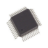
SLXT332QE.G2 Cortina Systems Inc, SLXT332QE.G2 Datasheet - Page 14

SLXT332QE.G2
Manufacturer Part Number
SLXT332QE.G2
Description
Manufacturer
Cortina Systems Inc
Datasheet
1.SLXT332QE.G2.pdf
(45 pages)
Specifications of SLXT332QE.G2
Operating Supply Voltage (typ)
5V
Screening Level
Industrial
Mounting
Surface Mount
Operating Supply Voltage (min)
4.75V
Operating Supply Voltage (max)
5.25V
Operating Temperature (min)
-40C
Operating Temperature (max)
85C
Lead Free Status / RoHS Status
Not Compliant
Available stocks
Company
Part Number
Manufacturer
Quantity
Price
Company:
Part Number:
SLXT332QE.G2
Manufacturer:
ICS
Quantity:
427
LXT332
Datasheet
249075, Revision 2.0
26 June 2007
Table 2
Table 3
Cortina Systems
1.
2. DI = Digital Input; DO = Digital Output; DI/O = Digital Input/Output; AI = Analog Input; AO = Analog Output; S = Power
1.
2. DI = Digital Input; DO = Digital Output; DI/O = Digital Input/Output; AI = Analog Input; AO = Analog Output; S = Power Supply.
QFP
Pin
QFP
39
40
41
42
43
44
Pin
1
2
3
4
5
6
7
35
36
37
Table 1
Supply.
Table 1
PLCC
describes the pins that do not change function in Unipolar Host mode and functions of pins unique to Bipolar mode.
describes the pins that do not change function in Unipolar Host mode and functions of pins unique to Bipolar mode.
Pin
10
12
13
11
1
2
3
4
5
6
7
8
9
PLCC
Pin
41
42
43
Unipolar Host Mode Pin Descriptions
Hardware Mode and Bipolar Hardware Mode Pin Descriptions
®
LXT332 Dual T1/E1 Line Interface Unit with Crystal-less Jitter Attenuation
(Bipolar)
(Bipolar)
(Bipolar)
(Bipolar)
Symbol
RNEG0
RPOS0
TRSTE
TPOS0
TNEG0
TCLK0
RCLK0
TAOS0
LEN20
LEN10
LEN00
MCLK
GND
Symbol
TDATA1
ECE1
BPV1
I/O
DO
DO
DO
DI
DI
DI
DI
DI
DI
DI
DI
DI
S
I/O
2
DO
DI
DI
Tristate Output Enable. When held High, forces all output pins to high
When held Low, Bipolar I/O mode is selected. In this mode, the framer interface is
bipolar (TPOS/TNEG and RPOS/RNEG), and the B8ZS/HDB3 encoders are disabled.
When clocked by MCLK, Unipolar I/O mode is selected. In this mode, the framer
interface is unipolar (TDATA and RDATA), and the TNEG and RNEG pins are
re
enable the B8ZS/HDB3 encoder/decoder for each port. The RNEG pins are re
as Bipolar Violation (BPV) indicators to report BPVs detected at the respective ports.
Transmit Clock
inputs are sampled on the falling edge of TCLK0.
Transmit Data Positive and Negative
the positive and negative sides of a bipolar input pair for port 0. Data to be transmitted
onto the port 0 twisted
Receive Data Positive and Negative
RNEG corresponds to receipt of a negative pulse on RTIP/RRING. A signal on RPOS
corresponds to receipt of a positive pulse on RTIP/RRING. RNEG/RPOS outputs are
Non Return
RCLK.
Receive Clock
Under Loss of Signal (LOS) conditions, RCLK0 is derived from MCLK.
Transmit All Ones Enable
TNEG or TDATA input is ignored and the port transmits a stream of ones at the TCLK
frequency. Refer to “Transmit All One’s” on
Line Length Equalizer
port 0 transmit pulse. See
Master Clock. The master clock (1.544 MHz for T1, 2.048 MHz for E1) must be
independent, free
that MCLK cannot be derived from RCLK because during a Loss of Signal (LOS)
condition, transceiver timing is based on MCLK.
Ground. Ground return for the VCC power supply.
2
-
mapped. The TNEG pins are re
Bipolar Violation
that a bipolar violation is detected at port 1.
Encoder Enable
B8ZS or HDB3 encoder/decoder for port 1.
Transmit Data
the twisted
-
to
-
-
Zero (NRZ). RPOS and RNEG are stable and valid on the rising edge of
pair line from port 1 is input at this pin.
-
-
Port 0. Normally, this clock is recovered from the port 0 input signal.
-
Port 0. 1.544 MHz for T1, 2.048 MHz for E1. The port 0 transmit data
running, continuously active and jitter free for receiver operation. Note
-
Port 1. In the Unipolar I/O mode, the data to be transmitted onto
-
-
-
pair line is input at these pins.
Port 1. In the Unipolar I/O mode, a High on this pin enables the
-
Port 1. In the Unipolar I/O mode, this pin goes High to indicate
Port 0. These pins determine the shape and amplitude of the
Table 5
-
1
Port 0. When TAOS is High and RLOOP is Low, the TPOS/
(Sheet 2 of 2)
for details.
-
mapped as Encoder Enables (ECE) to individually
Description
-
Description
-
Port 0. In the Bipolar I/O mode, a signal on
Port 0. In the Bipolar I/O mode, these pins are
page 25
3.0 Pin Assignments and Signal
for details.
1
(Sheet 1 of 3)
-
Z (tri
Descriptions
-
state).
-
mapped
Page 14


