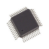
SLXT332QE.G2 Cortina Systems Inc, SLXT332QE.G2 Datasheet - Page 17

SLXT332QE.G2
Manufacturer Part Number
SLXT332QE.G2
Description
Manufacturer
Cortina Systems Inc
Datasheet
1.SLXT332QE.G2.pdf
(45 pages)
Specifications of SLXT332QE.G2
Operating Supply Voltage (typ)
5V
Screening Level
Industrial
Mounting
Surface Mount
Operating Supply Voltage (min)
4.75V
Operating Supply Voltage (max)
5.25V
Operating Temperature (min)
-40C
Operating Temperature (max)
85C
Lead Free Status / RoHS Status
Not Compliant
Available stocks
Company
Part Number
Manufacturer
Quantity
Price
Company:
Part Number:
SLXT332QE.G2
Manufacturer:
ICS
Quantity:
427
LXT332
Datasheet
249075, Revision 2.0
26 June 2007
4.0
4.1
Cortina Systems
Functional Description
Figure 1 on page 6
integrated Dual Line Interface Unit (DLIU) which contains two complete transceivers. The
DLIU is designed for both 1.544 Mbps (DSX-1) and 2.048 Mbps (E1) applications. Both
transceivers operate at the same frequency, which is determined by the MCLK input.
Each DLIU transceiver front end interfaces with two twisted-pair lines, one pair for
transmit, one pair for receive. These two twisted-pair lines comprise a digital data loop for
full duplex transmission. The integrated crystal-less jitter attenuator may be positioned in
either the transmit or receive path, or disabled.
Each DLIU transceiver back-end interfaces with a framer through either bipolar or unipolar
data I/O channels. The DLIU may be controlled by a microprocessor through the serial
port (Host mode), or by hard-wired pins for stand-alone operation (Hardware mode).
Receiver
The two receivers in the LXT332 are identical. The following paragraphs describe the
operation of one.
The twisted-pair input is received via a center-tapped 1:2 transformer. Positive pulses are
received at RTIP, negative pulses at RRING. Recovered data is output at RPOS and
RNEG in the bipolar mode and at RDATA in the unipolar mode. The recovered clock is
output at RCLK. RPOS/RNEG or RDATA outputs are valid on the rising edge of RCLK.
Refer to the Test Specifications Section for receiver timing.
The receive signal is processed through the peak detector and data slicers. The peak
detector samples the received signal and determines its maximum value. A percentage of
the peak value is provided to the data slicers as a threshold level to ensure optimum
signal-to-noise ratio. For DSX-1 applications (line length inputs LEN0 - LEN2 ≠ 000 or
001) the threshold is set to 70% (typical) of the peak value. This threshold is maintained
above the specified level for up to 15 successive zeros over the range of specified
operating conditions. For E1 applications (LEN inputs = 000 or 001), the threshold is 50%
(typical).
The receiver is capable of accurately recovering signals with up to -13.6 dB of attenuation
(from 2.4 V), corresponding to a received signal level of approximately 500 mV. Maximum
line length is 1500 feet of ABAM cable (approximately 6 dB of attenuation). Regardless of
received signal level, the peak detectors are held above a minimum level of 0.3 V (typical)
to provide immunity from impulsive noise.
After processing through the data slicers, the received signal goes to the data and timing
recovery section, and to the receive monitor. The data and timing recovery circuits provide
an input jitter tolerance better than required by Pub 62411 or ITU G.823, as shown in Test
Specifications.
The receiver monitor loads a digital counter at the RCLK frequency. The count is
incremented each time a zero is received, and reset to zero each time a one (mark) is
received. Upon receipt of 175 consecutive zeros the LOS flag is set, and the recovered
clock is replaced by MCLK at the RCLK output in a smooth transition. (MCLK is required
for receive operation.) When the received signal reaches 12.5% ones density (4 marks in
a sliding 32-bit period) with no more than 15 consecutive zeros, the LOS flag is reset and
another smooth transition replaces MCLK with the recovered clock at RCLK. During LOS
conditions, received data is output on RPOS/RNEG (or RDATA if unipolar I/O is selected).
®
LXT332 Dual T1/E1 Line Interface Unit with Crystal-less Jitter Attenuation
shows a simplified block diagram of the LXT332. The LXT332 is a fully
4.0 Functional Description
Page 17


