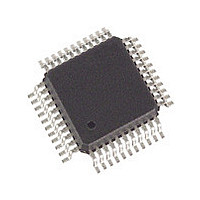
SLXT332QE.G2 Cortina Systems Inc, SLXT332QE.G2 Datasheet - Page 29

SLXT332QE.G2
Manufacturer Part Number
SLXT332QE.G2
Description
Manufacturer
Cortina Systems Inc
Datasheet
1.SLXT332QE.G2.pdf
(45 pages)
Specifications of SLXT332QE.G2
Operating Supply Voltage (typ)
5V
Screening Level
Industrial
Mounting
Surface Mount
Operating Supply Voltage (min)
4.75V
Operating Supply Voltage (max)
5.25V
Operating Temperature (min)
-40C
Operating Temperature (max)
85C
Lead Free Status / RoHS Status
Not Compliant
Available stocks
Company
Part Number
Manufacturer
Quantity
Price
Company:
Part Number:
SLXT332QE.G2
Manufacturer:
ICS
Quantity:
427
LXT332
Datasheet
249075, Revision 2.0
26 June 2007
4.9.5
Figure 13
4.10
Cortina Systems
QRSS Built-In Self Test - Host Mode
The QRSS Built -In Self Test (BIST) is available only under Host control. As shown in
Figure
Once the QRSS BIST function is selected, the VCQ0 and VCQ1 pins are re-mapped to
trigger the QRSS transmission. A High on one of these pins triggers QRSS pattern
transmission from the appropriate port. The QRSS pattern for DSX -1 systems is 2
with no more than 14 consecutive zeros. For CEPT systems the QRSS pattern is 2
The QRSS pattern is locked to MCLK. Once the QRSS transmission is activated, errors
can be inserted into the transmit data stream by causing a Low-to-High transition on the
TPOS/TDATA pin for the respective port.
In Bipolar I/O mode, Low-High transitions cause both a logic error and a bipolar violation
to be inserted into the QRSS data stream. In Unipolar I/O mode, only a logic error is
inserted.
The Pattern Detect circuitry is activated by the QRSS BIST function, although the basic
receive circuits are unaffected. The Pattern Detect pins (PD0 and PD1) indicate QRSS
pattern sync for the respective LIU port. The PD pin stays High until synchronization is
achieved on the QRSS pattern. The QRSS pattern is considered in sync when there are
fewer than 4 errors in 128 bits. The PD pin goes High indicating an out-of-sync condition if
4 or more errors are detected in 128 bits (i.e. sync is defined as fewer than 4 errors in
128 bits).
QRSS BIST
Initialization/Reset Operation
Upon initial power up, the transceiver is held static until the power supply reaches
approximately 3 V. Upon crossing this threshold, the device clears all internal registers
and begins calibration of the delay lines. A reference clock is required to calibrate the
delay lines. TCLK is the transmit reference, and MCLK is the receive reference. The PLLs
are continuously calibrated.
®
LXT332 Dual T1/E1 Line Interface Unit with Crystal-less Jitter Attenuation
13, the QRSS BIST function is selected by clocking the VCQE pin with MCLK.
TNEG
RCLK
RNEG
RPOS
MCLK
TPOS
TCLK
PD
(CLKE = 1)
RCLK
RCLK
(CLKE = 0)
PD
Receive QRSS
Pattern Lock
QRSS BIST =
QRSS Pattern Generator
QRSS Sync/Error Detector
3
3
Clocked
VCQE
Low
Recovery
Timing &
Timing
Control
-
to
VCQ0/1
-
High transition
Receive QRSS
Logic Error
Detected
TTIP
TRING
RTIP
RRING
4.10 Initialization/Reset
Operation
Page 29
20
15
-1,
-1.


