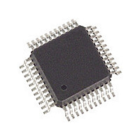
SLXT332QE.G2 Cortina Systems Inc, SLXT332QE.G2 Datasheet - Page 36

SLXT332QE.G2
Manufacturer Part Number
SLXT332QE.G2
Description
Manufacturer
Cortina Systems Inc
Datasheet
1.SLXT332QE.G2.pdf
(45 pages)
Specifications of SLXT332QE.G2
Operating Supply Voltage (typ)
5V
Screening Level
Industrial
Mounting
Surface Mount
Operating Supply Voltage (min)
4.75V
Operating Supply Voltage (max)
5.25V
Operating Temperature (min)
-40C
Operating Temperature (max)
85C
Lead Free Status / RoHS Status
Not Compliant
Available stocks
Company
Part Number
Manufacturer
Quantity
Price
Company:
Part Number:
SLXT332QE.G2
Manufacturer:
ICS
Quantity:
427
LXT332
Datasheet
249075, Revision 2.0
26 June 2007
6.0
Note:
Table 11
Table 12
Table 13
Cortina Systems
DC supply (referenced to GND)
Input voltage, any pin
Input current, any pin
Storage temperature
Caution:
1. Excluding RTIP and RRING which must stay between
2. Transient currents of up to 100 mA will not cause SCR latch
DC supply
Ambient operating temperature
1. Variation between TVCC0, TVCC1 and VCC must be within ±0.3 V of each other during steady state and transient
Total power dissipation – T1
(Maximum line length)
Total power dissipation – E1
High level input voltage
Low level input voltage
High level output voltage
Low level output voltage
1. Total power dissipation includes the device power consumption and load power dissipation while driving a 75
2. Functionality of pins depends on mode.
3. Output drivers will output CMOS logic levels into CMOS loads.
4. Except for MCLK, RTIP0, RRING0, RTIP1, and RRING1.
5. Applies to QFP pins 8, 11, 23 & 26; PLCC pins 14, 17, 29 & 32
current of 100 mA.
conditions.
secondary side. The T1 test circuit is a 100
without series resistors.
1
Parameter
Parameter
Parameter
Test Specifications
Information in
performance specifications of the LXT332 Dual Line Interface Unit and are guaranteed by
test, except as noted, by design.
Absolute Maximum Ratings
Recommended Operating Conditions
Electrical Characteristics (Over Recommended Operating Conditions)
(Sheet 1 of 2)
®
Operations at or beyond these limits may result in damage to the device.
Normal operation not guaranteed at these extremes.
LXT332 Dual T1/E1 Line Interface Unit with Crystal-less Jitter Attenuation
2
1
2,3
2,3
2,3
2,3
1
1
Table 11
Sym
VCC, TVCC0, TVCC1
Voh
Vih
Vol
Pd
Pd
Pd
Pd
Vil
VCC, TVCC0, TVCC1
through
Symbol
Ω
Min
line load connected to the driver outputs via a 1:1.15 turns ratio transformer
T
2.0
2.4
A
–
–
–
–
–
–
Symbol
T
V
I
STG
Table 17
IN
IN
-
6 V and V
Typ
700
550
575
490
–
–
–
–
-
up. TTIP, TRING, TV+, and TGND can withstand continuous
and
CC
Minimum
Max
900
700
700
600
0.8
0.4
4.75
+ 0.3 V.
-
–
–
40
Figure 17
GND
Minimum
-
-
10
65
–
Units
-
mW
mW
mW
mW
V
V
V
V
0.3
Typical
through
5.0
25
100% ones density
50% ones density
100% ones density
50% ones density
I
I
OUT
OUT
Maximum
=
= 1.6 mA
V
Figure 22
CC
-
+150
400 mA
6.0
10
+ 0.3
Test Conditions
Maximum
6.0 Test Specifications
5.25
85
represent the
Ω
load on the
Units
mA
°C
V
V
Units
Page 36
°C
V


