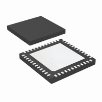
LMK03200ISQE/NOPB National Semiconductor, LMK03200ISQE/NOPB Datasheet - Page 14

LMK03200ISQE/NOPB
Manufacturer Part Number
LMK03200ISQE/NOPB
Description
IC CLOCK CONDITIONER PREC 48-LLP
Manufacturer
National Semiconductor
Type
Clock Conditionerr
Datasheet
1.LMK03200ISQENOPB.pdf
(40 pages)
Specifications of LMK03200ISQE/NOPB
Pll
Yes
Input
Clock
Output
LVDS, LVPECL
Number Of Circuits
1
Ratio - Input:output
1:9
Differential - Input:output
Yes/Yes
Frequency - Max
1.296GHz
Divider/multiplier
Yes/No
Voltage - Supply
3.15 V ~ 3.45 V
Operating Temperature
-40°C ~ 85°C
Mounting Type
Surface Mount
Package / Case
48-LLP
Frequency-max
1.296GHz
Lead Free Status / RoHS Status
Lead free / RoHS Compliant
Other names
LMK03200ISQETR
Available stocks
Company
Part Number
Manufacturer
Quantity
Price
Company:
Part Number:
LMK03200ISQE/NOPB
Manufacturer:
NSC
Quantity:
72
www.national.com
1.0 Functional Description
The LMK03200 family of precision clock conditioners com-
bine the functions of jitter cleaning/reconditioning, multiplica-
tion, and 0-delay distribution of a reference clock. The devices
integrate a Voltage Controlled Oscillator (VCO), a high per-
formance Integer-N Phase Locked Loop (PLL), a partially
integrated loop filter, three LVDS, and five LVPECL clock out-
put distribution blocks.
The devices include internal 3rd and 4th order poles to sim-
plify loop filter design and improve spurious performance. The
1st and 2nd order poles are off-chip to provide flexibility for
the design of various loop filter bandwidths.
The VCO output is optionally accessible on the Fout port. In-
ternally, the VCO output goes through a VCO divider to feed
the various clock distribution blocks.
Each clock distribution block includes a programmable di-
vider, a phase synchronization circuit, a programmable delay,
a clock output mux, and an LVDS or LVPECL output buffer.
This allows multiple integer-related and phase-adjusted
copies of the reference to be distributed to eight system com-
ponents.
The clock conditioners come in a 48-pin LLP package and are
footprint compatible with other clocking devices in the same
family.
1.1 BIAS PIN
To properly use the device, bypass Bias (pin 36) with a low
leakage 1 µF capacitor connected to Vcc. This is important
for low noise performance.
1.2 LDO BYPASS
To properly use the device, bypass LDObyp1 (pin 9) with a
10 µF capacitor and LDObyp2 (pin 10) with a 0.1 µF capacitor.
1.3 OSCILLATOR INPUT PORT (OSCin, OSCin*)
The purpose of OSCin is to provide the PLL with a reference
signal. Due to an internal DC bias the OSCin port should be
AC coupled, refer to the System Level Diagram in the Appli-
cation Information section. The OSCin port may be driven
single-endedly by AC grounding OSCin* with a 0.1 µF capac-
itor.
1.4 LOW NOISE, FULLY INTEGRATED VCO
The LMK03200 family of devices contain a fully integrated
VCO. For proper operation the VCO uses a frequency cali-
bration routine. The frequency calibration routine is activated
any time that the R15 register is programmed and
0_DELAY_MODE = 0. Once the frequency calibration routine
is run the temperature may not drift more than the maximum
allowable drift for continuous lock, ΔT
not guaranteed to stay in lock.
The status of the frequency calibration routine can be moni-
tored. See section
quence, with 0-Delay Mode
For the frequency calibration routine to work properly OSCin
must be driven by a valid signal and VCO_MUX = 0, otherwise
the resulting state is unknown.
2.2 Recommended Programing Se-
CL
, or else the VCO is
14
Refer to for a visual representation of what happens when
R15 is programmed.
1.5 LVDS/LVPECL OUTPUTS
By default all the clock outputs are disabled until pro-
grammed.
Each LVDS or LVPECL output may be disabled individually
by programming the CLKoutX_EN bits. All the outputs may
be disabled simultaneously by pulling the GOE pin low or
programming EN_CLKout_Global to 0.
The duty cycle of the LVDS and LVPECL clock outputs are
shown in the table below.
VCO_DIV
FIGURE 1. Frequency Calibration Routine Flowchart
2, 4, 6, 8
Any
3
5
7
Divided, or Divided and Delayed
Bypassed, or Delayed
Bypassed, or Delayed
Bypassed, or Delayed
CLKoutX_MUX
Any
30088741
Cycle
Duty
50%
50%
33%
40%
43%


