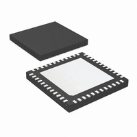
LMK03200ISQE/NOPB National Semiconductor, LMK03200ISQE/NOPB Datasheet - Page 16

LMK03200ISQE/NOPB
Manufacturer Part Number
LMK03200ISQE/NOPB
Description
IC CLOCK CONDITIONER PREC 48-LLP
Manufacturer
National Semiconductor
Type
Clock Conditionerr
Datasheet
1.LMK03200ISQENOPB.pdf
(40 pages)
Specifications of LMK03200ISQE/NOPB
Pll
Yes
Input
Clock
Output
LVDS, LVPECL
Number Of Circuits
1
Ratio - Input:output
1:9
Differential - Input:output
Yes/Yes
Frequency - Max
1.296GHz
Divider/multiplier
Yes/No
Voltage - Supply
3.15 V ~ 3.45 V
Operating Temperature
-40°C ~ 85°C
Mounting Type
Surface Mount
Package / Case
48-LLP
Frequency-max
1.296GHz
Lead Free Status / RoHS Status
Lead free / RoHS Compliant
Other names
LMK03200ISQETR
Available stocks
Company
Part Number
Manufacturer
Quantity
Price
Company:
Part Number:
LMK03200ISQE/NOPB
Manufacturer:
NSC
Quantity:
72
www.national.com
1.10 DIGITAL LOCK DETECT
The PLL digital lock detect circuitry compares the difference
between the phase of the inputs of the phase detector to a
RC generated delay of ε. To indicate a locked state the phase
error must be less than the ε RC delay for 5 consecutive ref-
erence cycles. Once in lock, the RC delay is changed to
approximately δ. To indicate an out of lock state, the phase
error must become greater δ. The values of ε and δ are shown
in the table below:
To utilize the digital lock detect feature, PLL_MUX must be
programmed for "Digital Lock Detect (Active High)" or "Digital
Lock Detect (Active Low)." When one of these modes is pro-
grammed the state of the LD pin will be set high or low as
determined by the description above as shown in
When the device is in power down mode and the LD pin is
programmed for a digital lock detect function, LD will show a
"no lock detected" condition which is low or high given active
high or active low circuitry respectively.
The accuracy of this circuit degrades at higher comparison
frequencies. To compensate for this, the DIV4 word should
be set to one if the comparison frequency exceeds 20 MHz.
The function of this word is to divide the comparison frequen-
cy presented to the lock detect circuit by 4.
10 ns
ε
20 ns
δ
Figure
3.
16
1.11 CLKout DELAYS
Each individual clock output includes a delay adjustment.
Clock output delay registers (CLKoutX_DLY) support a 150
ps step size and range from 0 to 2250 ps of total delay.
FIGURE 3. Digital Lock Detect Flowchart
30088705


