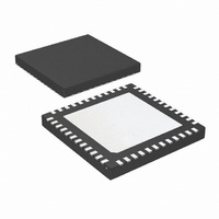
LMK03200ISQE/NOPB National Semiconductor, LMK03200ISQE/NOPB Datasheet - Page 34

LMK03200ISQE/NOPB
Manufacturer Part Number
LMK03200ISQE/NOPB
Description
IC CLOCK CONDITIONER PREC 48-LLP
Manufacturer
National Semiconductor
Type
Clock Conditionerr
Datasheet
1.LMK03200ISQENOPB.pdf
(40 pages)
Specifications of LMK03200ISQE/NOPB
Pll
Yes
Input
Clock
Output
LVDS, LVPECL
Number Of Circuits
1
Ratio - Input:output
1:9
Differential - Input:output
Yes/Yes
Frequency - Max
1.296GHz
Divider/multiplier
Yes/No
Voltage - Supply
3.15 V ~ 3.45 V
Operating Temperature
-40°C ~ 85°C
Mounting Type
Surface Mount
Package / Case
48-LLP
Frequency-max
1.296GHz
Lead Free Status / RoHS Status
Lead free / RoHS Compliant
Other names
LMK03200ISQETR
Available stocks
Company
Part Number
Manufacturer
Quantity
Price
Company:
Part Number:
LMK03200ISQE/NOPB
Manufacturer:
NSC
Quantity:
72
www.national.com
3.6 THERMAL MANAGEMENT
Power consumption of the LMK03200 family of devices can
be high enough to require attention to thermal management.
For reliability and performance reasons the die temperature
should be limited to a maximum of 125 °C. That is, as an es-
timate, T
sumption times θ
The package of the device has an exposed pad that provides
the primary heat removal path as well as excellent electrical
grounding to the printed circuit board. To maximize the re-
moval of heat from the package a thermal land pattern in-
cluding multiple vias to a ground plane must be incorporated
on the PCB within the footprint of the package. The exposed
pad must be soldered down to ensure adequate heat con-
duction out of the package. A recommended land and via
pattern can be downloaded from National's packaging web-
site. See LLP footprint gerbers at: http://www.national.com/
analog/packaging/gerber.
To minimize junction temperature it is recommended that a
simple heat sink be built into the PCB (if the ground plane
layer is not exposed). This is done by including a copper area
of about 2 square inches on the opposite side of the PCB from
the device. This copper area may be plated or solder coated
to prevent corrosion but should not have conformal coating (if
possible), which could provide thermal insulation. The vias
should top and bottom copper layers to the ground layer.
These vias act as “heat pipes” to carry the thermal energy
away from the device side of the board to where it can be more
effectively dissipated.
A
(ambient temperature) plus device power con-
JA
should not exceed 125 °C.
34
3.7 TERMINATION AND USE OF CLOCK OUTPUTS
(DRIVERS)
When terminating clock drivers keep in mind these guidelines
for optimum phase noise and jitter performance:
•
•
•
It is possible to drive a non-LVPECL or non-LVDS receiver
with a LVDS or LVPECL driver as long as the above guide-
lines are followed. Check the datasheet of the receiver or
input being driven to determine the best termination and cou-
pling method to be sure that the receiver is biased at its
optimum DC voltage (common mode voltage). For example,
when driving the OSCin/OSCin* input of the LMK03200 fam-
ily, OSCin/OSCin* should be AC coupled because OSCin/
OSCin* biases the signal to the proper DC level, see
6. This is only slightly different from the AC coupled cases
described in 3.7.2 because the DC blocking capacitors are
placed between the termination and the OSCin/OSCin* pins,
but the concept remains the same, which is the receiver (OS-
Cin/OSCin*) set the input to the optimum DC bias voltage
(common mode voltage), not the driver.
3.7.1 Termination for DC Coupled Differential Operation
For DC coupled operation of an LVDS driver, terminate with
100 Ω as close as possible to the LVDS receiver as shown in
Figure
the LVDS receiver.
For DC coupled operation of an LVPECL driver, terminate
with 50 Ω to Vcc - 2 V as shown in
terminate with a Thevenin equivalent circuit (120 Ω resistor
connected to Vcc and an 82 Ω resistor connected to ground
with the driver connected to the junction of the 120 Ω and 82
Ω resistors) as shown in
FIGURE 8. Differential LVDS Operation, DC Coupling
Transmission line theory should be followed for good
impedance matching to prevent reflections.
Clock drivers should be presented with the proper loads.
For example:
— LVDS drivers are current drivers and require a closed
— LVPECL drivers are open emitter and require a DC
Receivers should be presented with a signal biased to
their specified DC bias level (common mode voltage) for
proper operation. Some receivers have self-biasing inputs
that automatically bias to the proper voltage level. In this
case, the signal should normally be AC coupled.
current loop.
path to ground.
8. The LVDS driver will provide the DC bias level for
Figure 10
for Vcc = 3.3 V.
Figure
9. Alternatively
30088720
Figure


