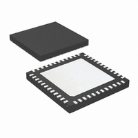
LMK03200ISQE/NOPB National Semiconductor, LMK03200ISQE/NOPB Datasheet - Page 25

LMK03200ISQE/NOPB
Manufacturer Part Number
LMK03200ISQE/NOPB
Description
IC CLOCK CONDITIONER PREC 48-LLP
Manufacturer
National Semiconductor
Type
Clock Conditionerr
Datasheet
1.LMK03200ISQENOPB.pdf
(40 pages)
Specifications of LMK03200ISQE/NOPB
Pll
Yes
Input
Clock
Output
LVDS, LVPECL
Number Of Circuits
1
Ratio - Input:output
1:9
Differential - Input:output
Yes/Yes
Frequency - Max
1.296GHz
Divider/multiplier
Yes/No
Voltage - Supply
3.15 V ~ 3.45 V
Operating Temperature
-40°C ~ 85°C
Mounting Type
Surface Mount
Package / Case
48-LLP
Frequency-max
1.296GHz
Lead Free Status / RoHS Status
Lead free / RoHS Compliant
Other names
LMK03200ISQETR
Available stocks
Company
Part Number
Manufacturer
Quantity
Price
Company:
Part Number:
LMK03200ISQE/NOPB
Manufacturer:
NSC
Quantity:
72
2.4.3 0_DELAY_MODE bit -- Activate 0-Delay Mode
This bit is only in register R0 and is used for activating the 0-
delay mode. Once the frequency calibration routine is com-
plete - as determined by monitoring the LD output in
DLD_MODE2 or waiting 2 ms after programming R15, this bit
may be set to activate 0-delay mode. Setting this bit sets the
N divider mux to use the feedback mux for input and prevents
the frequency calibration routine from activating when register
R15 is programmed. Once this bit is set and the 0-delay path
is completed, the PLL_N divider in register R15 will need to
be reprogrammed for final phase lock. See section
ommended Programing Sequence, with 0-Delay Mode
more information. Also refer to
back Mux
device for feedback of the selected signal.
2.4.4 FB_MUX [1:0] -- Feedback Mux
This bit is only in register R0 and is for use with the 0-delay
mode.
When using CLKout5 and FBCLKin/FBCLKin* for feedback
for 0-delay mode, the proper clock outputs must be enabled
to pass the feedback signal back to the N divider. Refer to the
table below for more details. The only requirement given by
the table below is that the clock output must be enabled with
CLKoutX_EN bits, if the clock is only used for feedback, the
clock does not need to be terminated which saves power. The
simplest feedback path to use is CLKout6 since it does not
require another CLKout to be enabled.
The electrical specification td
tion FB_MUX = 0 (CLKout5). If FB_MUX = 2 (CLKout6), then
td
Clock Feedback
0_DELAY_MODE
0-DELAY
FB_MUX [1:0]
FBCLKin*
FBCLKin/
CLKout 5
CLKout 6
0 (default)
Source
, OSCin to CLKoutX 0-delay, increases 100 ps.
0
1
2
3
for more information on proper configuration of the
1
CLKout5_EN
(See 2.4.9)
Don't care
Calibration
Frequency
Disabled
FBCLKin/FBCLKin* Input
Routine
Enabled
0-DELAY
1
1
CLKout5 (default)
2.4.4 FB_MUX [1:0] -- Feed-
Reserved
CLKout6
is given with the condi-
Mode
CLKout6_EN
N divider mux
Feedback Mux
(See 2.4.9)
VCO Divider
(Ndiv Mux)
(FB_MUX)
1
1
1
2.2 Rec-
for
25
2.4.5 VCO_MUX [1:0] -- VCO Mux
This bit is only in register R7 and is used to select either the
VCO divider output or the VCO output for the clock distribution
path. By selecting the VCO output (VCO_MUX=2), the VCO
divider is bypassed allowing a higher frequency at the channel
divider inputs, which can be used to generate output frequen-
cies not allowable otherwise.
Important: The VCO calibration routine requires that the VCO
divider (VCO_MUX = 0) is selected when programming R15.
The VCO divider (VCO_MUX=0) must be selected for the
VCO calibration routine to operate properly.
Important: When bypassing the VCO divider (VCO_MUX=2),
0-delay mode may not be used. However 0_DELAY_MODE
is set to 1 when re-programming PLL_N after the VCO divider
has been bypassed to prevent the frequency calibration rou-
tine from running. The new PLL_N value = Old PLL_N * VCO
divider. Once PLL_N is re-programmed 0_DELAY_MODE is
set back to 0. See the programming section,
mended Programming Sequence, bypassing VCO
more information.
2.4.6 CLKoutX_MUX [1:0] -- Clock Output Multiplexers
These bits control the Clock Output Multiplexer for each clock
output. Changing between the different modes changes the
blocks in the signal path and therefore incurs a delay relative
to the bypass mode. The different MUX modes and associ-
ated delays are listed below.
CLKoutX_MUX
VCO_MUX [1:0]
[1:0]
0
1
2
3
0
1
2
3
Divided and
Bypassed
(default)
Delayed
Delayed
Divided
Mode
VCO Divider (default)
Reserved
Reserved
Added Delay Relative
Mode
programmed delay)
programmed delay)
VCO
to Bypass Mode
(In addition to the
(In addition to the
100 ps
400 ps
500 ps
0 ps
2.3 Recom-
www.national.com
divider, for


