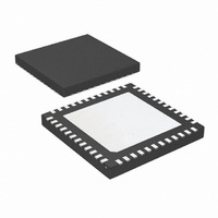
LMK03200ISQE/NOPB National Semiconductor, LMK03200ISQE/NOPB Datasheet - Page 17

LMK03200ISQE/NOPB
Manufacturer Part Number
LMK03200ISQE/NOPB
Description
IC CLOCK CONDITIONER PREC 48-LLP
Manufacturer
National Semiconductor
Type
Clock Conditionerr
Datasheet
1.LMK03200ISQENOPB.pdf
(40 pages)
Specifications of LMK03200ISQE/NOPB
Pll
Yes
Input
Clock
Output
LVDS, LVPECL
Number Of Circuits
1
Ratio - Input:output
1:9
Differential - Input:output
Yes/Yes
Frequency - Max
1.296GHz
Divider/multiplier
Yes/No
Voltage - Supply
3.15 V ~ 3.45 V
Operating Temperature
-40°C ~ 85°C
Mounting Type
Surface Mount
Package / Case
48-LLP
Frequency-max
1.296GHz
Lead Free Status / RoHS Status
Lead free / RoHS Compliant
Other names
LMK03200ISQETR
Available stocks
Company
Part Number
Manufacturer
Quantity
Price
Company:
Part Number:
LMK03200ISQE/NOPB
Manufacturer:
NSC
Quantity:
72
1.12 GLOBAL DELAYS
After the N divider and R divider are two delays PLL_N_DLY
and PLL_R_DLY. They support a 150 ps step size and range
from 0 to 2250 ps of total delay. When using the 0-delay
mode, these delays can be used to cause the clock outputs
to lead or lag the clock input phase.
use of the global delays. Note, it is possible to use the indi-
vidual delays on each clock output (CLKoutX_DLY) to further
1.13 VCO DIVIDER BYPASS MODE
Once the LMK03200 is locked, the VCO divider may be by-
passed to allow a higher frequency at the channel divider
inputs, which can be used to generate output frequencies not
allowable otherwise. The VCO_DIV bypass mode does not
work with 0-delay mode. See programming information in
sections
passing VCO divider
Mux. SYNC* is not used when in VCO divider bypass mode.
1.14 0-DELAY MODE
The LMK03200 family can feedback an output to the phase
detector either internally using CLKout5 or CLKout6, or ex-
ternally by routing any clock output back to the FBCLKin/
FBCLKin* input port to be synchronized with the reference
clock for 0-delay output.
To ensure 0-delay for all the outputs, the lowest frequency
output must be feed back to the PLL. This requirement forces
the maximum phase detector frequency
output frequency.
When CLKout5 or CLKout6 is used for feedback internally,
CLKout5 or CLKout6 are still valid for regular clocking appli-
cations. If CLKout5 or CLKout6 are unused, they do not need
to be externally terminated, by not terminating the output
power consumption is reduced.
To engage the 0-delay mode, refer to programming instruc-
tions in section
with 0-Delay
Figure 5
More detail is in section
quence, with 0-Delay Mode
illustrates the 0-delay mode programming sequence.
2.3 Recommended Programming Sequence, by-
Mode.
2.2 Recommended Programing Sequence,
and
2.2 Recommended Programing Se-
2.4.5 VCO_MUX [1:0] -- VCO
Figure 4
≤
the minimum clock
illustrates the
FIGURE 4. Global Lead and Lag
17
alter the phase of the various clock outputs. This is not shown
in
and PLL_R_DLY to shift clock outputs to lead or lag the ref-
erence input phase. It doesn't reflect exact timing or account
for delays in buffers internal to the device, meaning the clock
output is not guaranteed to have 0 phase delay from the ref-
erence input to a clock output as shown at the pins of the
device.
The 0-delay mode may not be used together with the
VCO_DIV bypass except for the purpose of being temporarily
enabled to re-program the PLL_N to keep the PLL in lock. See
2.3 Recommended Programming Sequence, bypassing VCO
divider
Figure
FIGURE 5. Outline of 0-delay mode programming
for more information.
4. Note that
Figure 4
sequence
30088711
illustrates use of PLL_N_DLY
30088742
www.national.com


