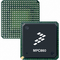
MPC8241LZQ200D Freescale Semiconductor, MPC8241LZQ200D Datasheet - Page 15

MPC8241LZQ200D
Manufacturer Part Number
MPC8241LZQ200D
Description
IC MPU 32BIT 200MHZ PPC 357-PBGA
Manufacturer
Freescale Semiconductor
Datasheet
1.MPC8241LZQ200D.pdf
(58 pages)
Specifications of MPC8241LZQ200D
Processor Type
MPC82xx PowerQUICC II 32-bit
Speed
200MHz
Voltage
1.8V
Mounting Type
Surface Mount
Package / Case
357-PBGA
Family Name
MPC82XX
Device Core
PowerQUICC II
Device Core Size
32b
Frequency (max)
200MHz
Instruction Set Architecture
RISC
Supply Voltage 1 (typ)
1.8V
Operating Supply Voltage (max)
1.9V
Operating Supply Voltage (min)
1.7V
Operating Temp Range
0C to 105C
Operating Temperature Classification
Commercial
Mounting
Surface Mount
Pin Count
357
Package Type
BGA
Lead Free Status / RoHS Status
Contains lead / RoHS non-compliant
Features
-
Lead Free Status / Rohs Status
Not Compliant
Available stocks
Company
Part Number
Manufacturer
Quantity
Price
Company:
Part Number:
MPC8241LZQ200D
Manufacturer:
FREESCALE
Quantity:
513
Company:
Part Number:
MPC8241LZQ200D
Manufacturer:
Freescale Semiconductor
Quantity:
10 000
Part Number:
MPC8241LZQ200D
Manufacturer:
FREESCALE
Quantity:
20 000
Figure 6
DLL locking range loop delay versus frequency of operation.
Freescale Semiconductor
At recommended operating conditions (see
Notes:
1. Rise and fall times for the PCI_SYNC_IN input are measured from 0.4 through 2.4 V.
2. Specification value at maximum frequency of operation.
3. Pin-to-pin skew includes quantifying the additional amount of clock skew (or jitter) from the DLL besides any intentional skew
4. Relock time is guaranteed by design and characterization. Relock time is not tested.
5. Relock timing is guaranteed by design. PLL-relock time is the maximum amount of time required for PLL lock after a stable
6. DLL_EXTEND is bit 7 of the PMC2 register <72>. N is a non-zero integer (see
7. Rise and fall times for the OSC_IN input are guaranteed by design and characterization. OSC_IN input rise and fall times are
Num
added to the clocking signals from the variable length DLL synchronization feedback loop, that is, the amount of variance
between the internal sys_logic_clk and the SDRAM_SYNC_IN signal after the DLL is locked. While pin-to-pin skew between
SDRAM_CLKs can be measured, the relationship between the internal sys_logic_clk and the external SDRAM_SYNC_IN
cannot be measured and is guaranteed by design.
V
disabled and subsequently re-enabled during sleep mode. Also note that HRST_CPU/HRST_CTRL must be held asserted
for a minimum of 255 bus clocks after the PLL-relock time during the reset sequence.
of one SDRAM_SYNC_OUT clock cycle in ns. T
board runner) from SDRAM_SYNC_OUT to SDRAM_SYNC_IN in ns; 6.25 inches of loop length (unloaded PC board runner)
corresponds to approximately 1 ns of delay. For details about how
Freescale application note AN2164, MPC8245/MPC8241 Memory Clock Design Guidelines, for details on MPC8241 memory
clock design.
not tested.
21
DD
and PCI_SYNC_IN are reached during the reset sequence. This specification also applies when the PLL has been
shows the PCI_SYNC_IN input clock timing diagram, and
OSC_IN frequency stability
PCI_SYNC_IN
Characteristics and Conditions
MPC8241 Integrated Processor Hardware Specifications, Rev. 10
Table 8. Clock AC Timing Specifications (continued)
Figure 6. PCI_SYNC_IN Input Clock Timing Diagram
VM
Table
5a
2) with LV
VM = Midpoint Voltage (1.4 V)
1
loop
VM
DD
is the propagation delay of the DLL synchronization feedback loop (PC
= 3.3 V ± 0.3 V
5b
VM
Figure 7
CV
IL
Min
through
—
CV
Figure 7
Figure 7
IH
2
Figure 10
through
Electrical and Thermal Characteristics
through
Max
100
may be used, refer to the
Figure
Figure 10
10). T
Unit
ppm
clk
3
is the period
show the
Notes
15


