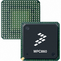
MPC8241LZQ200D Freescale Semiconductor, MPC8241LZQ200D Datasheet - Page 24

MPC8241LZQ200D
Manufacturer Part Number
MPC8241LZQ200D
Description
IC MPU 32BIT 200MHZ PPC 357-PBGA
Manufacturer
Freescale Semiconductor
Datasheet
1.MPC8241LZQ200D.pdf
(58 pages)
Specifications of MPC8241LZQ200D
Processor Type
MPC82xx PowerQUICC II 32-bit
Speed
200MHz
Voltage
1.8V
Mounting Type
Surface Mount
Package / Case
357-PBGA
Family Name
MPC82XX
Device Core
PowerQUICC II
Device Core Size
32b
Frequency (max)
200MHz
Instruction Set Architecture
RISC
Supply Voltage 1 (typ)
1.8V
Operating Supply Voltage (max)
1.9V
Operating Supply Voltage (min)
1.7V
Operating Temp Range
0C to 105C
Operating Temperature Classification
Commercial
Mounting
Surface Mount
Pin Count
357
Package Type
BGA
Lead Free Status / RoHS Status
Contains lead / RoHS non-compliant
Features
-
Lead Free Status / Rohs Status
Not Compliant
Available stocks
Company
Part Number
Manufacturer
Quantity
Price
Company:
Part Number:
MPC8241LZQ200D
Manufacturer:
FREESCALE
Quantity:
513
Company:
Part Number:
MPC8241LZQ200D
Manufacturer:
Freescale Semiconductor
Quantity:
10 000
Part Number:
MPC8241LZQ200D
Manufacturer:
FREESCALE
Quantity:
20 000
Electrical and Thermal Characteristics
Figure 14
24
Notes:
1. All PCI signals are measured from GV
2. All memory and related interface output signal specifications are specified from the VM = 1.4 V of the rising edge of the
3. PCI bused signals are composed of the following signals: LOCK, IRDY, C/BE[3:0], PAR, TRDY, FRAME, STOP, DEVSEL,
4. To meet minimum output hold specifications relative to PCI_SYNC_IN for both 33- and 66-MHz PCI systems, the MPC8241
Num
GV
memory bus clock, sys_logic_clk to the TTL level (0.8 or 2.0 V) of the signal in question. sys_logic_clk is the same as
PCI_SYNC_IN in 1:1 mode, but is twice the frequency in 2:1 mode (processor/memory bus clock rising edges occur on every
rising and falling edge of PCI_SYNC_IN). See
PERR, SERR, AD[31:0], REQ[4:0], GNT[4:0], IDSEL, and INTA.
has a programmable output hold delay for PCI signals (the PCI_SYNC_IN to output valid timing is also affected). The initial
value of the output hold delay is determined by the values on the MCP and CKE reset configuration signals; the values on
these two signals are inverted and subsequently stored as the initial settings of PCI_HOLD_DEL = PMCR2[5, 4] (power
management configuration register 2 <0x72>), respectively. Because MCP and CKE have internal pull-up resistors, the
default value of PCI_HOLD_DEL after reset is 0b00. Additional output hold delay values are available by programming the
PCI_HOLD_DEL value of the PMCR2 configuration register. See
hold time.
14b
DD
_OV
sys_logic_clk to output high impedance (for all others)
provides the AC test load for the MPC8241.
DD
of the signal in question for 3.3 V PCI signaling levels. See
Output
MPC8241 Integrated Processor Hardware Specifications, Rev. 10
Table 11. Output AC Timing Specifications (continued)
Figure 14. AC Test Load for the MPC8241
Characteristic
DD
Z
0
_OV
= 50 Ω
Output Measurements are Made at the Device Pin
DD
Figure
/2 of the rising edge of PCI_SYNC_IN to 0.285 × GV
11.
Figure 15
R
L
= 50 Ω
Figure
for PCI_HOLD_DEL effect on output valid and
12.
GV
PCI or Memory
DD
Min
—
_OV
DD
/2 for
Max
Freescale Semiconductor
4.0
DD
_OV
DD
Unit
ns
or 0.615 ×
Notes
2


