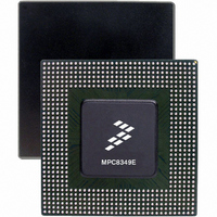
MPC8349ECVVAGDB Freescale Semiconductor, MPC8349ECVVAGDB Datasheet - Page 13

MPC8349ECVVAGDB
Manufacturer Part Number
MPC8349ECVVAGDB
Description
IC MPU POWERQUICC II 672-TBGA
Manufacturer
Freescale Semiconductor
Datasheet
1.MPC8349EVVAJFB.pdf
(87 pages)
Specifications of MPC8349ECVVAGDB
Processor Type
MPC83xx PowerQUICC II Pro 32-Bit
Speed
400MHz
Voltage
1.2V
Mounting Type
Surface Mount
Package / Case
672-TBGA
For Use With
MPC8349E-MITX-GP - KIT REFERENCE PLATFORM MPC8349EMPC8349E-MITXE - BOARD REFERENCE FOR MPC8349MPC8349EA-MDS-PB - KIT MODULAR DEV SYSTEM MPC8349E
Lead Free Status / RoHS Status
Lead free / RoHS Compliant
Features
-
Available stocks
Company
Part Number
Manufacturer
Quantity
Price
Company:
Part Number:
MPC8349ECVVAGDB
Manufacturer:
FREESCALE
Quantity:
8
Company:
Part Number:
MPC8349ECVVAGDB
Manufacturer:
Freescale Semiconductor
Quantity:
10 000
4.3
Table 8
5
This section describes the DC and AC electrical specifications for the reset initialization timing and
electrical requirements of the MPC8349EA.
5.1
Table 9
Freescale Semiconductor
At recommended operating conditions with LV
EC_GTX_CLK125 frequency
EC_GTX_CLK125 cycle time
EC_GTX_CLK rise and fall time
EC_GTX_CLK125 duty cycle
EC_GTX_CLK125 jitter
Notes:
1. Rise and fall times for EC_GTX_CLK125 are measured from 0.5 and 2.0 V for LV
2. EC_GTX_CLK125 is used to generate the GTX clock for the eTSEC transmitter with 2% degradation. The EC_GTX_CLK125
Input high voltage
Input low voltage
Input current
Output high voltage
Output low voltage
LV
duty cycle can be loosened from 47%/53% as long as the PHY device can tolerate the duty cycle generated by the eTSEC
GTX_CLK. See
reference clock.
DD
= 3.3 V.
RESET Initialization
provides the TSEC gigabit reference clocks (EC_GTX_CLK125) AC timing specifications.
provides the DC electrical characteristics for the RESET pins of the MPC8349EA.
TSEC Gigabit Reference Clock Timing
RESET DC Electrical Characteristics
MPC8349EA PowerQUICC II Pro Integrated Host Processor Hardware Specifications, Rev. 12
1000Base-T for RGMII, RTBI
Parameter
Section 8.2.4, “RGMII and RTBI AC Timing Specifications
2
Parameter
LV
LV
Table 8. EC_GTX_CLK125 AC Timing Specifications
Table 9. RESET Pins DC Electrical Characteristics
DD
DD
GMII, TBI
= 2.5 V
= 3.3 V
DD
= 2.5 ± 0.125 mV/ 3.3 V ± 165 mV
t
G125R
t
G125H
Symbol
t
t
G125
G125
—
/t
/t
G125F
G125
Symbol
V
V
V
V
I
OH
IN
OL
IH
IL
Min
45
47
—
—
—
—
I
OH
I
OL
Condition
= –8.0 mA
= 8.0 mA
—
—
—
for the duty cycle for 10Base-T and 100Base-T
Typical
125
—
—
—
8
DD
= 2.5 V and from 0.6 and 2.7 V for
–0.3
Min
2.0
2.4
—
—
1
±150
Max
0.75
1.0
55
53
—
—
OV
DD
Max
0.8
0.5
±5
—
RESET Initialization
MHz
Unit
+ 0.3
ns
ns
ps
%
Notes
Unit
μA
—
—
V
V
V
V
1
2
2
13


