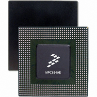
MPC8349ECVVAGDB Freescale Semiconductor, MPC8349ECVVAGDB Datasheet - Page 9

MPC8349ECVVAGDB
Manufacturer Part Number
MPC8349ECVVAGDB
Description
IC MPU POWERQUICC II 672-TBGA
Manufacturer
Freescale Semiconductor
Datasheet
1.MPC8349EVVAJFB.pdf
(87 pages)
Specifications of MPC8349ECVVAGDB
Processor Type
MPC83xx PowerQUICC II Pro 32-Bit
Speed
400MHz
Voltage
1.2V
Mounting Type
Surface Mount
Package / Case
672-TBGA
For Use With
MPC8349E-MITX-GP - KIT REFERENCE PLATFORM MPC8349EMPC8349E-MITXE - BOARD REFERENCE FOR MPC8349MPC8349EA-MDS-PB - KIT MODULAR DEV SYSTEM MPC8349E
Lead Free Status / RoHS Status
Lead free / RoHS Compliant
Features
-
Available stocks
Company
Part Number
Manufacturer
Quantity
Price
Company:
Part Number:
MPC8349ECVVAGDB
Manufacturer:
FREESCALE
Quantity:
8
Company:
Part Number:
MPC8349ECVVAGDB
Manufacturer:
Freescale Semiconductor
Quantity:
10 000
Figure 3
3.3-V signals, respectively.
2.1.3
Table 3
preliminary estimates.
2.2
The device does not require the core supply voltage and I/O supply voltages to be applied in any particular
order. Note that during the power ramp up, before the power supplies are stable, there may be a period of
time that I/O pins are actively driven. After the power is stable, as long as PORESET is asserted, most I/O
pins are three-stated. To minimize the time that I/O pins are actively driven, it is recommended to apply
core voltage before I/O voltage and assert PORESET before the power supplies fully ramp up.
Freescale Semiconductor
Local bus interface utilities signals
PCI signals (not including PCI output clocks)
PCI output clocks (including PCI_SYNC_OUT)
DDR signal
DDR2 signal
TSEC/10/100 signals
DUART, system control, I
GPIO signals
provides information on the characteristics of the output driver strengths. The values are
shows the undershoot and overshoot voltage of the PCI interface of the MPC8349EA for the
Power Sequencing
MPC8349EA PowerQUICC II Pro Integrated Host Processor Hardware Specifications, Rev. 12
Output Driver Characteristics
Figure 3. Maximum AC Waveforms on PCI Interface for 3.3-V Signaling
Driver Type
Undervoltage
Overvoltage
2
Waveform
Waveform
C, JTAG, USB
Table 3. Output Drive Capability
11 ns
(Min)
4 ns
(Max)
36 (half-strength mode)
Output Impedance
62.5 ns
4 ns
(Max)
(Ω)
+7.1 V
+3.6 V
–3.5 V
40
25
40
18
18
40
40
40
0 V
7.1 V p-to-p
7.1 V p-to-p
(Min)
(Min)
LV
LV
GV
GV
OV
Electrical Characteristics
OV
OV
DD
DD
Voltage
Supply
DD
DD
DD
DD
DD
= 2.5/3.3 V
= 2.5/3.3 V
= 3.3 V,
= 3.3 V
= 2.5 V
= 1.8 V
= 3.3 V
9


