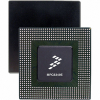
MPC8349ECVVAGDB Freescale Semiconductor, MPC8349ECVVAGDB Datasheet - Page 67

MPC8349ECVVAGDB
Manufacturer Part Number
MPC8349ECVVAGDB
Description
IC MPU POWERQUICC II 672-TBGA
Manufacturer
Freescale Semiconductor
Datasheet
1.MPC8349EVVAJFB.pdf
(87 pages)
Specifications of MPC8349ECVVAGDB
Processor Type
MPC83xx PowerQUICC II Pro 32-Bit
Speed
400MHz
Voltage
1.2V
Mounting Type
Surface Mount
Package / Case
672-TBGA
For Use With
MPC8349E-MITX-GP - KIT REFERENCE PLATFORM MPC8349EMPC8349E-MITXE - BOARD REFERENCE FOR MPC8349MPC8349EA-MDS-PB - KIT MODULAR DEV SYSTEM MPC8349E
Lead Free Status / RoHS Status
Lead free / RoHS Compliant
Features
-
Available stocks
Company
Part Number
Manufacturer
Quantity
Price
Company:
Part Number:
MPC8349ECVVAGDB
Manufacturer:
FREESCALE
Quantity:
8
Company:
Part Number:
MPC8349ECVVAGDB
Manufacturer:
Freescale Semiconductor
Quantity:
10 000
As shown in
loop (PLL) and the clock unit to create the coherent system bus clock (csb_clk), the internal clock for the
DDR controller (ddr_clk), and the internal clock for the local bus interface unit (lbiu_clk).
The csb_clk frequency is derived from a complex set of factors that can be simplified into the following
equation:
In PCI host mode, PCI_SYNC_IN × (1 + CFG_CLKIN_DIV) is the CLKIN frequency.
The csb_clk serves as the clock input to the e300 core. A second PLL inside the e300 core multiplies the
csb_clk frequency to create the internal clock for the e300 core (core_clk). The system and core PLL
multipliers are selected by the SPMF and COREPLL fields in the reset configuration word low (RCWL),
which is loaded at power-on reset or by one of the hard-coded reset options. See the chapter on reset,
clocking, and initialization in the MPC8349EA Reference Manual for more information on the clock
subsystem.
The internal ddr_clk frequency is determined by the following equation:
ddr_clk is not the external memory bus frequency; ddr_clk passes through the DDR clock divider (÷2) to
create the differential DDR memory bus clock outputs (MCK and MCK). However, the data rate is the
same frequency as ddr_clk.
The internal lbiu_clk frequency is determined by the following equation:
lbiu_clk is not the external local bus frequency; lbiu_clk passes through the LBIU clock divider to create
the external local bus clock outputs (LSYNC_OUT and LCLK[0:2]). The LBIU clock divider ratio is
controlled by LCCR[CLKDIV].
In addition, some of the internal units may have to be shut off or operate at lower frequency than the
csb_clk frequency. Those units have a default clock ratio that can be configured by a memory-mapped
register after the device exits reset.
Freescale Semiconductor
TSEC1
TSEC2, I
Security core
USB DR, USB MPH
PCI1, PCI2 and DMA complex
csb_clk = {PCI_SYNC_IN × (1 + CFG_CLKIN_DIV)} × SPMF
ddr_clk = csb_clk × (1 + RCWL[DDRCM])
lbiu_clk = csb_clk × (1 + RCWL[LBIUCM])
2
C1
MPC8349EA PowerQUICC II Pro Integrated Host Processor Hardware Specifications, Rev. 12
Figure
Unit
40, the primary clock input (frequency) is multiplied up by the system phase-locked
Table 56
Table 56. Configurable Clock Units
Default Frequency
specifies which units have a configurable clock frequency.
csb_clk/3
csb_clk/3
csb_clk/3
csb_clk/3
csb_clk
Off, csb_clk, csb_clk/2, csb_clk/3
Off, csb_clk, csb_clk/2, csb_clk/3
Off, csb_clk, csb_clk/2, csb_clk/3
Off, csb_clk, csb_clk/2, csb_clk/3
Off, csb_clk
Options
Clocking
67


