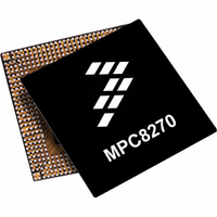
MPC8270VVUPEA Freescale Semiconductor, MPC8270VVUPEA Datasheet - Page 22

MPC8270VVUPEA
Manufacturer Part Number
MPC8270VVUPEA
Description
IC MPU POWERQUICC II 480-TBGA
Manufacturer
Freescale Semiconductor
Series
PowerQUICC IIr
Datasheet
1.MPC8270VRMIBA.pdf
(80 pages)
Specifications of MPC8270VVUPEA
Processor Type
MPC82xx PowerQUICC II 32-bit
Speed
450MHz
Voltage
1.5V
Mounting Type
Surface Mount
Package / Case
480-TBGA
Processor Series
MPC8xxx
Core
603e
Data Bus Width
32 bit
Maximum Clock Frequency
450 MHz
Operating Supply Voltage
0 V to 3 V
Maximum Operating Temperature
+ 105 C
Data Ram Size
32 KB
Program Memory Size
16 KB
Program Memory Type
EPROM/Flash
Core Size
32 Bit
Cpu Speed
450MHz
Embedded Interface Type
I2C, JTAG, SPI, UART
Digital Ic Case Style
TBGA
No. Of Pins
480
Rohs Compliant
Yes
Lead Free Status / RoHS Status
Lead free / RoHS Compliant
Features
-
Lead Free Status / Rohs Status
Lead free / RoHS Compliant
Available stocks
Company
Part Number
Manufacturer
Quantity
Price
Company:
Part Number:
MPC8270VVUPEA
Manufacturer:
FREESCAL
Quantity:
105
Company:
Part Number:
MPC8270VVUPEA
Manufacturer:
FREESCAL
Quantity:
748
Company:
Part Number:
MPC8270VVUPEA
Manufacturer:
Freescale Semiconductor
Quantity:
10 000
Part Number:
MPC8270VVUPEA
Manufacturer:
NXP/恩智浦
Quantity:
20 000
AC Electrical Characteristics
6.3 JTAG Timings
Table 14
22
JTAG external clock frequency of operation
JTAG external clock cycle time
JTAG external clock pulse width measured at 1.4V
JTAG external clock rise and fall times
TRST assert time
Input setup times
lists the JTAG timings.
Figure 12
The UPM machine outputs change on the internal tick determined by the memory
controller programming; the AC specifications are relative to the internal tick. The
SDRAM and GPCM machine outputs change on CLKin’s rising edge.
1:2, 1:3, 1:4, 1:5, 1:6
CLKin
CLKin
CLKin
PLL Clock Ratio
Parameter
Figure 12. Internal Tick Spacing for Memory Controller Signals
MPC8280 PowerQUICC™ II Family Hardware Specifications, Rev. 1.8
1:2.5
1:3.5
is a representation of the information in
T1
T1
T1
Table 13. Tick Spacing for Memory Controller Signals
Boundary-scan data
T2
T2
T2
1/4 CLKin
3/10 CLKin
4/14 CLKin
Tick Spacing (T1 Occurs at the Rising Edge of CLKin)
Table 14. JTAG Timings
TMS, TDI
T3
T3
T3
T2
NOTE
t
Symbol
T4
JTGR
t
t
t
JTDVKH
JTKHKL
JTIVKH
T4
t
t
T4
f
t
TRST
JTGF
1/2 CLKin
1/2 CLKin
1/2 CLKin
JTG
JTG
and
2
Table
T3
1
Min
13.
30
15
25
0
0
4
4
for 1:2, 1:3, 1:4, 1:5, 1:6
for 1:2.5
for 1:3.5
3/4 CLKin
8/10 CLKin
11/14 CLKin
Max
33.3
—
—
—
—
—
5
T4
Freescale Semiconductor
MHz
Unit
ns
ns
ns
ns
ns
ns
Notes
3
4
4
,
,
,
6
6
7
7


