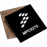
MPC8270VVUPEA Freescale Semiconductor, MPC8270VVUPEA Datasheet - Page 5

MPC8270VVUPEA
Manufacturer Part Number
MPC8270VVUPEA
Description
IC MPU POWERQUICC II 480-TBGA
Manufacturer
Freescale Semiconductor
Series
PowerQUICC IIr
Datasheet
1.MPC8270VRMIBA.pdf
(80 pages)
Specifications of MPC8270VVUPEA
Processor Type
MPC82xx PowerQUICC II 32-bit
Speed
450MHz
Voltage
1.5V
Mounting Type
Surface Mount
Package / Case
480-TBGA
Processor Series
MPC8xxx
Core
603e
Data Bus Width
32 bit
Maximum Clock Frequency
450 MHz
Operating Supply Voltage
0 V to 3 V
Maximum Operating Temperature
+ 105 C
Data Ram Size
32 KB
Program Memory Size
16 KB
Program Memory Type
EPROM/Flash
Core Size
32 Bit
Cpu Speed
450MHz
Embedded Interface Type
I2C, JTAG, SPI, UART
Digital Ic Case Style
TBGA
No. Of Pins
480
Rohs Compliant
Yes
Lead Free Status / RoHS Status
Lead free / RoHS Compliant
Features
-
Lead Free Status / Rohs Status
Lead free / RoHS Compliant
Available stocks
Company
Part Number
Manufacturer
Quantity
Price
Company:
Part Number:
MPC8270VVUPEA
Manufacturer:
FREESCAL
Quantity:
105
Company:
Part Number:
MPC8270VVUPEA
Manufacturer:
FREESCAL
Quantity:
748
Company:
Part Number:
MPC8270VVUPEA
Manufacturer:
Freescale Semiconductor
Quantity:
10 000
Part Number:
MPC8270VVUPEA
Manufacturer:
NXP/恩智浦
Quantity:
20 000
Freescale Semiconductor
•
•
•
•
— Uses the local bus signals, removing need for additional pins
System interface unit (SIU)
— Clock synthesizer
— Reset controller
— Real-time clock (RTC) register
— Periodic interrupt timer
— Hardware bus monitor and software watchdog timer
— IEEE 1149.1 JTAG test access port
12-bank memory controller
— Glueless interface to SRAM, page mode SDRAM, DRAM, EPROM, Flash and other user- definable
— Byte write enables and selectable parity generation
— 32-bit address decodes with programmable bank size
— Three user-programmable machines, general-purpose chip-select machine, and page-mode pipeline
— Byte selects for 64-bus width (60x) and byte selects for 32-bus width (local)
— Dedicated interface logic for SDRAM
CPU core can be disabled and the device can be used in slave mode to an external core
Communications processor module (CPM)
— Embedded 32-bit communications processor (CP) uses a RISC architecture for flexible support for
— Interfaces to G2_LE core through an on-chip 32-Kbyte dual-port data RAM, an on-chip 32-Kbyte
— Serial DMA channels for receive and transmit on all serial channels
— Parallel I/O registers with open-drain and interrupt capability
— Virtual DMA functionality executing memory-to-memory and memory-to-I/O transfers
— Three fast communications controllers supporting the following protocols:
— Two multichannel controllers (MCCs) (one MCC on the MPC8270)
peripherals
SDRAM machine
communications protocols
dual-port instruction RAM and DMA controller
– 10/100-Mbit Ethernet/IEEE 802.3 CDMA/CS interface through media independent interface (MII)
– ATM—Full-duplex SAR protocols at 155 Mbps, through UTOPIA interface, AAL5, AAL1, AAL0
– Transparent
– HDLC—Up to T3 rates (clear channel)
– FCC2 can also be connected to the TC layer (MPC8280 only)
– Each MCC handles 128 serial, full-duplex, 64-Kbps data channels. Each MCC can be split into four
– Almost any combination of subgroups can be multiplexed to single or multiple TDM interfaces up
or reduced media independent interface (RMII)
protocols, TM 4.0 CBR, VBR, UBR, ABR traffic types, up to 64 K external connections (no ATM
support for the MPC8270)
subgroups of 32 channels each.
to four TDM interfaces per MCC
MPC8280 PowerQUICC™ II Family Hardware Specifications, Rev. 1.8
Overview
5


