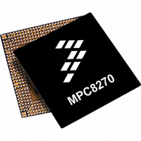
MPC8270VVUPEA Freescale Semiconductor, MPC8270VVUPEA Datasheet - Page 78

MPC8270VVUPEA
Manufacturer Part Number
MPC8270VVUPEA
Description
IC MPU POWERQUICC II 480-TBGA
Manufacturer
Freescale Semiconductor
Series
PowerQUICC IIr
Datasheet
1.MPC8270VRMIBA.pdf
(80 pages)
Specifications of MPC8270VVUPEA
Processor Type
MPC82xx PowerQUICC II 32-bit
Speed
450MHz
Voltage
1.5V
Mounting Type
Surface Mount
Package / Case
480-TBGA
Processor Series
MPC8xxx
Core
603e
Data Bus Width
32 bit
Maximum Clock Frequency
450 MHz
Operating Supply Voltage
0 V to 3 V
Maximum Operating Temperature
+ 105 C
Data Ram Size
32 KB
Program Memory Size
16 KB
Program Memory Type
EPROM/Flash
Core Size
32 Bit
Cpu Speed
450MHz
Embedded Interface Type
I2C, JTAG, SPI, UART
Digital Ic Case Style
TBGA
No. Of Pins
480
Rohs Compliant
Yes
Lead Free Status / RoHS Status
Lead free / RoHS Compliant
Features
-
Lead Free Status / Rohs Status
Lead free / RoHS Compliant
Available stocks
Company
Part Number
Manufacturer
Quantity
Price
Company:
Part Number:
MPC8270VVUPEA
Manufacturer:
FREESCAL
Quantity:
105
Company:
Part Number:
MPC8270VVUPEA
Manufacturer:
FREESCAL
Quantity:
748
Company:
Part Number:
MPC8270VVUPEA
Manufacturer:
Freescale Semiconductor
Quantity:
10 000
Part Number:
MPC8270VVUPEA
Manufacturer:
NXP/恩智浦
Quantity:
20 000
Document Revision History
78
Revision
1.0
2/2004
Date
MPC8280 PowerQUICC™ II Family Hardware Specifications, Rev. 1.8
• Removal of “Advance Information” and “Preliminary.” The MPC8280 is fully qualified.
•
•
• Section 1.1: Core frequency range is 166–450 MHz
• Addition of ZQ (516 PBGA with Lead spheres) package references
•
• Note following
•
•
•
•
•
• Sections 4.1–4.5: New
•
•
•
•
• Section 6.2: Addition of Note: CLKIN Jitter and Duty Cycle
•
•
•
•
•
•
•
• Addition of “Note: Temperature Reflow for the VR Package" on page 59
•
•
•
•
•
Table
Figure
Table
Table
Table
Table
Table
Table
Table
Table
Table
Table
Table
Table
Table 16
to corresponding values in tables.
Table
Table
Table
Table
Table
Table
PA6—FCC2_UT_RXADDR3
PA7—FCC2_UT_TXADDR3
PA8—FCC2_UT_TXADDR4
PB14—RXD3
PC19—SPICLK
PC22—FCC1_UT_TXPRTY
PC28—FCC2_UT_RXADDR4
Table
PA[6–9], PB[8–17, 20–25], PC[6–7, 10–13], PD[4, 10–13, 16, 23–28]
Table
Table
Table 25. Document Revision History (continued)
1: New
4: VDD and VCCSYN modified to 1.45–1.60 V
5: Addition of note 2 regarding TRST and PORESET (see VIH row of
5: Changed I
5: Moved QREQ to V
5: Addition of critical interrupt (CINT) to IRQ5 for V
6: Addition of Ψ
7: Modified power values (+ 150mW to each)
8: Addition of note 2. Changed PCI impedance to 27 Ω.
9: Changes to sp36b, SP38a, sp38b, sp37a, sp39a, sp40 and sp41
10: Changes to sp16a, sp18a, sp20 and sp21
11: Changes to sp13 @ 66 and 83 MHz, sp14 @ 83 MHz
12: Change to sp30 (data bus signals). Changes to sp33b. Removal of note 2.
21: Addition of note 1 to TRST (AH3) and PORESET (AG6)
21: Addition of RXD3 to CPM port pin PB14. Previously omitted.
21: Addition of critical interrupt (CINT) to B21 and U4. Previously omitted.
21: Addition of note 5 to ‘No connect’ (AA1, AG4)
23: Addition of note 1 to TRST (F22) and PORESET (B25)
23: Addition of previously omitted signals that are multiplexed with CPM port pins:
23: Removal of serial interface 1 (SI1) signals from port pins (see note 2 in
23: Addition of critical interrupt (CINT) to AC1 and B14. Previously omitted.
23: Addition of note 5 to ‘No connect’ (E17, C23)
1: Modification to note 2
through
Table
Table
OL
4: Modified
JT
for 60x signals to 6.0 mA
20: Modification of note 1 regarding CPU and CPM Fmin. Modification
and note 4
OL
: I
OL
Substantive Changes
= 3.2 mA
OL
(I
OL
= 6.0mA)
Freescale Semiconductor
Table
Figure
5)
1):


