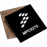
MPC8270VVUPEA Freescale Semiconductor, MPC8270VVUPEA Datasheet - Page 79

MPC8270VVUPEA
Manufacturer Part Number
MPC8270VVUPEA
Description
IC MPU POWERQUICC II 480-TBGA
Manufacturer
Freescale Semiconductor
Series
PowerQUICC IIr
Datasheet
1.MPC8270VRMIBA.pdf
(80 pages)
Specifications of MPC8270VVUPEA
Processor Type
MPC82xx PowerQUICC II 32-bit
Speed
450MHz
Voltage
1.5V
Mounting Type
Surface Mount
Package / Case
480-TBGA
Processor Series
MPC8xxx
Core
603e
Data Bus Width
32 bit
Maximum Clock Frequency
450 MHz
Operating Supply Voltage
0 V to 3 V
Maximum Operating Temperature
+ 105 C
Data Ram Size
32 KB
Program Memory Size
16 KB
Program Memory Type
EPROM/Flash
Core Size
32 Bit
Cpu Speed
450MHz
Embedded Interface Type
I2C, JTAG, SPI, UART
Digital Ic Case Style
TBGA
No. Of Pins
480
Rohs Compliant
Yes
Lead Free Status / RoHS Status
Lead free / RoHS Compliant
Features
-
Lead Free Status / Rohs Status
Lead free / RoHS Compliant
Available stocks
Company
Part Number
Manufacturer
Quantity
Price
Company:
Part Number:
MPC8270VVUPEA
Manufacturer:
FREESCAL
Quantity:
105
Company:
Part Number:
MPC8270VVUPEA
Manufacturer:
FREESCAL
Quantity:
748
Company:
Part Number:
MPC8270VVUPEA
Manufacturer:
Freescale Semiconductor
Quantity:
10 000
Part Number:
MPC8270VVUPEA
Manufacturer:
NXP/恩智浦
Quantity:
20 000
Freescale Semiconductor
Revision
0.3
0.2
0.1
11/2002
6/2003
Date
—
Table
Initial public release
MPC8280 PowerQUICC™ II Family Hardware Specifications, Rev. 1.8
• Removal of notes stating “no local bus” on VR-package devices. The MPC8270VR and the
• References to “G2 core” changed to “G2_LE core.” Refer to the G2 Core Reference Manual
• Addition of VCCSYN to “Note” below
•
•
•
•
•
•
•
•
• Section 6.2: Addition of note on PCI timing
•
• Addition of statement before clock tables about selection of clock configuration and input
•
MPC8275VR have local bus support.
(G2CORERM/D).
Figure
Table
Table
Table
Table
Table
Table
current note 2.
Figure
Table
operating frequencies
frequency
Table 21
23, “VR Pinout”: Addition of C18 to the Ground (GND) pin list (page 63)
Table 25. Document Revision History (continued)
5: Addition of note 1
6: Addition of θ
7: Addition of various configurations, Modification of values. Addition of note 3.
9: Addition of 66 MHZ and 100 MHz values. Addition of sp42a/sp43a.
10: Addition of 66 MHZ and 100 MHz values
12: sp30 values. sp33b @100 MHz value. Removal of previous note 2. Modification of
16,
2: New
5,
and
Figure
Table
Table
17,
6,
Figure
Table
23: Addition of note 1 to CPM pins
JB
and θ
18,
7, and
JC
Table
. Modifications to ZU package values.
Figure
Substantive Changes
19,
Table
Table
8: Addition of notes
4, and to note 3 of
20: Addition of note 1 concerning minimum
Table 5
Document Revision History
79


