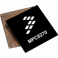
MPC8270VVUPEA Freescale Semiconductor, MPC8270VVUPEA Datasheet - Page 4

MPC8270VVUPEA
Manufacturer Part Number
MPC8270VVUPEA
Description
IC MPU POWERQUICC II 480-TBGA
Manufacturer
Freescale Semiconductor
Series
PowerQUICC IIr
Datasheet
1.MPC8270VRMIBA.pdf
(80 pages)
Specifications of MPC8270VVUPEA
Processor Type
MPC82xx PowerQUICC II 32-bit
Speed
450MHz
Voltage
1.5V
Mounting Type
Surface Mount
Package / Case
480-TBGA
Processor Series
MPC8xxx
Core
603e
Data Bus Width
32 bit
Maximum Clock Frequency
450 MHz
Operating Supply Voltage
0 V to 3 V
Maximum Operating Temperature
+ 105 C
Data Ram Size
32 KB
Program Memory Size
16 KB
Program Memory Type
EPROM/Flash
Core Size
32 Bit
Cpu Speed
450MHz
Embedded Interface Type
I2C, JTAG, SPI, UART
Digital Ic Case Style
TBGA
No. Of Pins
480
Rohs Compliant
Yes
Lead Free Status / RoHS Status
Lead free / RoHS Compliant
Features
-
Lead Free Status / Rohs Status
Lead free / RoHS Compliant
Available stocks
Company
Part Number
Manufacturer
Quantity
Price
Company:
Part Number:
MPC8270VVUPEA
Manufacturer:
FREESCAL
Quantity:
105
Company:
Part Number:
MPC8270VVUPEA
Manufacturer:
FREESCAL
Quantity:
748
Company:
Part Number:
MPC8270VVUPEA
Manufacturer:
Freescale Semiconductor
Quantity:
10 000
Part Number:
MPC8270VVUPEA
Manufacturer:
NXP/恩智浦
Quantity:
20 000
Overview
4
•
•
•
•
•
•
— High-performance (SPEC95 benchmark at 450 MHz; 855 Dhrystones MIPS at 450 MHz)
— Supports bus snooping for data cache coherency
— Floating-point unit (FPU)
Separate power supply for internal logic and for I/O
Separate PLLs for G2_LE core and for the CPM
— G2_LE core and CPM can run at different frequencies for power/performance optimization
— Internal core/bus clock multiplier that provides 2:1, 2.5:1, 3:1, 3.5:1, 4:1, 4.5:1, 5:1, 6:1, 7:1, 8:1 ratios
— Internal CPM/bus clock multiplier that provides 2:1, 2.5:1, 3:1, 3.5:1, 4:1, 5:1, 6:1, 8:1 ratios
64-bit data and 32-bit address 60x bus
— Bus supports multiple master designs
— Supports single- and four-beat burst transfers
— 64-, 32-, 16-, and 8-bit port sizes controlled by on-chip memory controller
— Supports data parity or ECC and address parity
32-bit data and 18-bit address local bus
— Single-master bus, supports external slaves
— Eight-beat burst transfers
— 32-, 16-, and 8-bit port sizes controlled by on-chip memory controller
60x-to-PCI bridge
— Programmable host bridge and agent
— 32-bit data bus, 66.67/83.3/100 MHz, 3.3 V
— Synchronous and asynchronous 60x and PCI clock modes
— All internal address space available to external PCI host
— DMA for memory block transfers
— PCI-to-60x address remapping
PCI bridge
— PCI Specification Revision 2.2 compliant and supports frequencies up to 66 MHz
— On-chip arbitration
— Support for PCI-to-60x-memory and 60x-memory-to-PCI streaming
— PCI host bridge or periphera
— Includes 4 DMA channels for the following transfers:
— Includes all of the configuration registers (which are automatically loaded from the EPROM and used
— Supports the I
— Hot-swap friendly (supports the hot swap specification as defined by PICMG 2.1 R1.0 August 3, 1998)
— Support for 66.67/83.33/100 MHz, 3.3 V specification
— 60x-PCI bus core logic that uses a buffer pool to allocate buffers for each port
– PCI-to-60x to 60x-to-PCI
– 60x-to-PCI to PCI-to-60x
– PCI-to-60x to PCI-to-60x
– 60x-to-PCI to 60x-to-PCI
to configure the MPC8280) required by the PCI standard as well as message and doorbell registers
MPC8280 PowerQUICC™ II Family Hardware Specifications, Rev. 1.8
2
O standard
l
capabilities
Freescale Semiconductor


