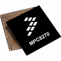
MPC8270VVUPEA Freescale Semiconductor, MPC8270VVUPEA Datasheet - Page 7

MPC8270VVUPEA
Manufacturer Part Number
MPC8270VVUPEA
Description
IC MPU POWERQUICC II 480-TBGA
Manufacturer
Freescale Semiconductor
Series
PowerQUICC IIr
Datasheet
1.MPC8270VRMIBA.pdf
(80 pages)
Specifications of MPC8270VVUPEA
Processor Type
MPC82xx PowerQUICC II 32-bit
Speed
450MHz
Voltage
1.5V
Mounting Type
Surface Mount
Package / Case
480-TBGA
Processor Series
MPC8xxx
Core
603e
Data Bus Width
32 bit
Maximum Clock Frequency
450 MHz
Operating Supply Voltage
0 V to 3 V
Maximum Operating Temperature
+ 105 C
Data Ram Size
32 KB
Program Memory Size
16 KB
Program Memory Type
EPROM/Flash
Core Size
32 Bit
Cpu Speed
450MHz
Embedded Interface Type
I2C, JTAG, SPI, UART
Digital Ic Case Style
TBGA
No. Of Pins
480
Rohs Compliant
Yes
Lead Free Status / RoHS Status
Lead free / RoHS Compliant
Features
-
Lead Free Status / Rohs Status
Lead free / RoHS Compliant
Available stocks
Company
Part Number
Manufacturer
Quantity
Price
Company:
Part Number:
MPC8270VVUPEA
Manufacturer:
FREESCAL
Quantity:
105
Company:
Part Number:
MPC8270VVUPEA
Manufacturer:
FREESCAL
Quantity:
748
Company:
Part Number:
MPC8270VVUPEA
Manufacturer:
Freescale Semiconductor
Quantity:
10 000
Part Number:
MPC8270VVUPEA
Manufacturer:
NXP/恩智浦
Quantity:
20 000
2 Operating Conditions
Table 3
Table 4
Freescale Semiconductor
•
•
1
2
3
4
1
2
Core supply voltage
PLL supply voltage
I/O supply voltage
Input voltage
Junction temperature
Storage temperature range
Core supply voltage
PLL supply voltage
I/O supply voltage
Input voltage
Junction temperature (maximum)
Ambient temperature
guaranteed. Stress beyond those listed may affect device reliability or cause permanent damage.
that VDD/VCCSYN should be raised before or simultaneous with VDDH during power-on reset. VDD/VCCSYN may
exceed VDDH by more than 0.4 V during power-on reset for no more than 100 ms.
should not exceed VDD/VCCSYN by more than 2.5 V during normal operation.
is not guaranteed.
Caution: These are the recommended and tested operating conditions. Proper operation outside of these conditions
Absolute maximum ratings are stress ratings only; functional operation (see
Caution: VDD/VCCSYN must not exceed VDDH by more than 0.4 V during normal operation. It is recommended
Caution: VDDH can exceed VDD/VCCSYN by 3.3 V during power on reset by no more than 100 mSec. VDDH
Caution: VIN must not exceed VDDH by more than 2.5 V at any time, including during power-on reset.
Note that for extended temperature parts the range is (-40)
shows the maximum electrical ratings.
lists recommended operational voltage conditions.
— Eight independent baud rate generators and 20 input clock pins for supplying clocks to FCCs, SCCs,
— Four independent 16-bit timers that can be interconnected as two 32-bit timers
Inverse multiplexing for ATM capabilities (IMA) (MPC8280 only).Supported by eight transfer transmission
convergence (TC) layers between the TDMs and FCC2.
Transmission convergence (TC) layer (MPC8280 only)
– Supports T1, CEPT, T1/E1, T3/E3, pulse code modulation highway, ISDN basic rate, ISDN primary
SMCs, and serial channels
rate, Freescale interchip digital link (IDL), general circuit interface (GCI), and user-defined TDM
serial interfaces
4
Rating
Rating
3
2
2
MPC8280 PowerQUICC™ II Family Hardware Specifications, Rev. 1.8
Table 4. Recommended Operating Conditions
Table 3. Absolute Maximum Ratings
VCCSYN
VCCSYN
Symbol
Symbol
VDDH
VDDH
VDD
T
VIN
VDD
VIN
T
T
STG
T
A
j
j
T A
– 105
GND (-0.3) – 3.465
GND(-0.3) – 3.6
T j
3.135 – 3.465
(-55) – (+150)
1.45 – 1.60
1.45 – 1.60
.
-0.3 – 2.25
-0.3 – 2.25
-0.3 – 4.0
0–70
Value
Value
105
120
2
2
Table
1
4) at the maximums is not
1
Operating Conditions
Unit
Unit
°C
°C
°C
°C
V
V
V
V
V
V
V
V
7


