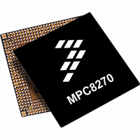
MPC8270VVUPEA Freescale Semiconductor, MPC8270VVUPEA Datasheet - Page 3

MPC8270VVUPEA
Manufacturer Part Number
MPC8270VVUPEA
Description
IC MPU POWERQUICC II 480-TBGA
Manufacturer
Freescale Semiconductor
Series
PowerQUICC IIr
Datasheet
1.MPC8270VRMIBA.pdf
(80 pages)
Specifications of MPC8270VVUPEA
Processor Type
MPC82xx PowerQUICC II 32-bit
Speed
450MHz
Voltage
1.5V
Mounting Type
Surface Mount
Package / Case
480-TBGA
Processor Series
MPC8xxx
Core
603e
Data Bus Width
32 bit
Maximum Clock Frequency
450 MHz
Operating Supply Voltage
0 V to 3 V
Maximum Operating Temperature
+ 105 C
Data Ram Size
32 KB
Program Memory Size
16 KB
Program Memory Type
EPROM/Flash
Core Size
32 Bit
Cpu Speed
450MHz
Embedded Interface Type
I2C, JTAG, SPI, UART
Digital Ic Case Style
TBGA
No. Of Pins
480
Rohs Compliant
Yes
Lead Free Status / RoHS Status
Lead free / RoHS Compliant
Features
-
Lead Free Status / Rohs Status
Lead free / RoHS Compliant
Available stocks
Company
Part Number
Manufacturer
Quantity
Price
Company:
Part Number:
MPC8270VVUPEA
Manufacturer:
FREESCAL
Quantity:
105
Company:
Part Number:
MPC8270VVUPEA
Manufacturer:
FREESCAL
Quantity:
748
Company:
Part Number:
MPC8270VVUPEA
Manufacturer:
Freescale Semiconductor
Quantity:
10 000
Part Number:
MPC8270VVUPEA
Manufacturer:
NXP/恩智浦
Quantity:
20 000
Figure 1
1.1 Features
The major features of the MPC8280 are as follows:
Freescale Semiconductor
•
MCC1
Notes:
1
2
3
MPC8280 only (not on MPC8270, the VR package, nor the ZQ package)
MPC8280 has 2 serial interface (SI) blocks and 8 TDM ports. MPC8270 and the VR and ZQ packages have
MPC8280, MPC8275VR, MPC8275ZQ only (not on MPC8270, MPC8270VR, nor MPC8270ZQ)
Parallel I/O
Generators
Baud Rate
Dual-issue integer (G2_LE) core
— A core version of the EC603e microprocessor
— System core microprocessor supporting frequencies of 166–450 MHz
— Separate 16-Kbyte data and instruction caches:
— Architecture-compliant memory management unit (MMU)
— Common on-chip processor (COP) test interface
Timers
1
only 1 SI block and 4 TDM ports (TDM2[A–D]).
shows the block diagram. Shaded portions are device-specific; refer to the notes below.
G2_LE Core
MCC2
– Four-way set associative
– Physically addressed
– LRU replacement algorithm
FCC1
Communication Processor Module (CPM)
TC Layer Hardware1
Controller
8 TDM Ports2
Interrupt
32-bit RISC Microcontroller
MPC8280 PowerQUICC™ II Family Hardware Specifications, Rev. 1.8
FCC2
and Program ROM
FCC3
Instruction
32 KB
16 Kbytes
16 Kbytes
RAM
D-Cache
I-Cache
D-MMU
I-MMU
SCC1
Figure 1. MPC8280 Block Diagram
Microcode
32 KB
Data
RAM
SCC2
IMA
3 MII or RMII
1
SCC3
Ports
Time Slot Assigner
Serial Interface2
4 Virtual
IDMAs
DMAs
Serial
SCC4/
USB
2 UTOPIA
Ports3
SMC1
System Interface Unit
SMC2
Memory Controller
Bus Interface Unit
System Functions
Clock Counter
60x-to-Local
60x-to-PCI
Non-Multiplexed
Bridge
Bridge
(SIU)
SPI
I/O
I
2
C
32 bits, up to 100 MHz
32 bits, up to 66 MHz
60x Bus
Local Bus
PCI Bus
or
Overview
3


