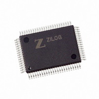
Z8018008FSG Zilog, Z8018008FSG Datasheet - Page 15

Z8018008FSG
Manufacturer Part Number
Z8018008FSG
Description
IC 8MHZ Z180 CMOS ENH MPU 80-QFP
Manufacturer
Zilog
Datasheet
1.Z8018006PSG.pdf
(85 pages)
Specifications of Z8018008FSG
Processor Type
Z180
Features
8-Bit, Enhanced Z80 Megacell
Speed
8MHz
Voltage
5V
Mounting Type
Surface Mount
Package / Case
80-BQFP
Processor Series
Z8018xx
Core
Z80
Data Bus Width
8 bit
Maximum Clock Frequency
8 MHz
Number Of Timers
2
Operating Supply Voltage
0 V to 5 V
Maximum Operating Temperature
+ 70 C
Mounting Style
SMD/SMT
Minimum Operating Temperature
0 C
Lead Free Status / RoHS Status
Lead free / RoHS Compliant
Other names
269-3882
Z8018008FSG
Z8018008FSG
Available stocks
Company
Part Number
Manufacturer
Quantity
Price
PS014004-1106
BUSACK
device, the MPU address and data bus, and some control signals that enter their high-imped-
ance state.
BUSREQ
external devices (such as DMA controllers) to request access to the
system bus. This request demands a higher priority than
end of the current machine cycle. This signal stops the CPU from executing further instruc-
tions and places address and data buses, and other control signals, into the high-impedance
state.
CKA0, CKA1—
mode, these pins are the transmit and receive clock
outputs from the ASCI baud rate generators. When in input mode, these pins serve as the
external clock inputs for the ASCI baud rate generators.
and
CKS—
CLOCK—
reference clock for the MPU and the external system. The
frequency of this output is equal to one-half that of the crystal or input clock frequency.
CTS0–CTS1—
signals for the ASCI channels.
multiplexed with
D0–D7—
constitute an 8-bit bidirectional data bus, used for the transfer of
information to and from I/O and memory devices. The data bus enters the high-impedance
state during reset and external bus acknowledge cycles.
DCD0—
for ASCI channel 0.
DREQ0, DREQ1. DMA Request 0 and 1 (input, active Low).
DMA transfer from one of the on-chip DMA channels. The DMA channels monitor these
inputs to determine when an external device is ready for a
inputs can be programmed to be either level or edge sensed.
CKA0
E—
transactions.
EXTAL—
external clock can be input to the Z80180 on this pin when a crystal is not used. This input is
Schmitt-triggered.
HALT
either the
Enable Clock (output, active High). Synchronous machine cycle clock output during bus
CKA1
.
—
Serial Clock (bidirectional, active High). This line is the clock for the
Data Carrier Detect 0 (input, active Low). A programmable modem control signal
HALT/SLEEP
Data Bus (bidirectional, active High, 3-state).
—Bus Acknowledge (output, active Low).
—Bus Request (input, active Low). This input is used by
External Clock Crystal (input, active High). Crystal oscillator connections. An
HALT
System Clock (output, active High). The output is used as a
is multiplexed with
Clear to send
Asynchronous Clock 0 and 1 (bidirectional, active High). When in output
or
RXS
SLEEP
.
(output, active Low). This output is asserted after the CPU executes
instruction, and is waiting for either nonmaskable or maskable
0
TEND0
and
CTS1
1
(inputs, active Low). These lines are modem control
is
.
BUSACK
D0–D7
NMI
CKA0
READ
DREQ0
and is always recognized at the
DREQ
indicates the requesting
is multiplexed with
or
WRITE
Microprocessor Unit
is multiplexed with
is used to request a
operation. These
CSIO
Overview
DREQ0
channel.
Z80180
,
9


