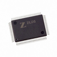
Z8018008FSG Zilog, Z8018008FSG Datasheet - Page 51

Z8018008FSG
Manufacturer Part Number
Z8018008FSG
Description
IC 8MHZ Z180 CMOS ENH MPU 80-QFP
Manufacturer
Zilog
Datasheet
1.Z8018006PSG.pdf
(85 pages)
Specifications of Z8018008FSG
Processor Type
Z180
Features
8-Bit, Enhanced Z80 Megacell
Speed
8MHz
Voltage
5V
Mounting Type
Surface Mount
Package / Case
80-BQFP
Processor Series
Z8018xx
Core
Z80
Data Bus Width
8 bit
Maximum Clock Frequency
8 MHz
Number Of Timers
2
Operating Supply Voltage
0 V to 5 V
Maximum Operating Temperature
+ 70 C
Mounting Style
SMD/SMT
Minimum Operating Temperature
0 C
Lead Free Status / RoHS Status
Lead free / RoHS Compliant
Other names
269-3882
Z8018008FSG
Z8018008FSG
Available stocks
Company
Part Number
Manufacturer
Quantity
Price
ASCI Status Register 0, 1 (STAT0, 1)
ASCI Status Registers
PS014004-1106
Note:
Each channel status register allows interrogation of ASCI communication, error and modem
control signal status, and enabling or disabling of ASCI interrupts.
RDRF: Receive Data Register Full (bit 7)—
byte is loaded into an empty
RDRF
mode, during
OVRN: Overrun Error (bit 6)—An overrun condition occurs when the receiver finishes
assembling a character, but the
However, this status bit is not set until the most recent character received before the overrun
becomes the oldest byte in the FIFO. This bit is cleared when software writes a
bit in the
pin is auto enabled and is negated (High).
When an overrun occurs, the receiver does not place the character in the shift register into
the FIFO, nor any subsequent characters, until the last good character comes to the top of the
FIFO so that
PE: Parity Error (bit 5)—A parity error is detected when parity checking is enabled by
the
parity does not match the
until or unless the error character becomes the oldest one in the
software writes a
mode, and for ASCI0 if the
Bit
Bit
MOD1
RDRF
RDRF
is cleared to
R
R
7
7
If a framing or parity error occurs,
generated the error) is still loaded into the FIFO.
CNTLA
ASCI Status Register 0 (STAT0: I/O Address = 04h)
ASCI Status Register 1 (STAT1: I/O Address = 05h)
bit in the
OVRN
OVRN
OVRN
RESET
R
6
R
6
register, and also by
1
0
to the
is set, and software then writes a
Figure 34. ASCI Status Registers
CNT1LA
by reading
and for ASCI0 if the
PE
PE
R
R
5
5
EFR
PEO
DCD0
RxFIFO
register being
FE
FE
4
R
4
bit in the
R
bit in the
RxFIFO
RDR
pin is auto-enabled and is negated (High).
.
R/W
R/W
and most recent character in the FIFO from
RE
RE
3
RESET
3
is full so that there is no room for the character.
CNTRLA
CNTLB
DCD0
1
DCD
, and a character is assembled in which the
, in
R
__
RDRF
2
2
0
register. However, this status bit is not set
input is auto-enabled and is negated (High).
IOSTOP
register, and also by
RDRF
TDRE
TDRE
is still set and the receive data (which
1
R
R
1
1
to
is set to
EFR
mode, and for ASCI0 if the
R/W
TIE
R/W
TIE
to clear it.
0
0
RxFIFO
1
when an incoming data
Microprocessor Unit
RESET
.
PE
is cleared when
, in
1
Architecture
to the
IOSTOP
IOSTOP
Z80180
DCD0
EFR
45


