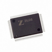
Z8018008FSG Zilog, Z8018008FSG Datasheet - Page 53

Z8018008FSG
Manufacturer Part Number
Z8018008FSG
Description
IC 8MHZ Z180 CMOS ENH MPU 80-QFP
Manufacturer
Zilog
Datasheet
1.Z8018006PSG.pdf
(85 pages)
Specifications of Z8018008FSG
Processor Type
Z180
Features
8-Bit, Enhanced Z80 Megacell
Speed
8MHz
Voltage
5V
Mounting Type
Surface Mount
Package / Case
80-BQFP
Processor Series
Z8018xx
Core
Z80
Data Bus Width
8 bit
Maximum Clock Frequency
8 MHz
Number Of Timers
2
Operating Supply Voltage
0 V to 5 V
Maximum Operating Temperature
+ 70 C
Mounting Style
SMD/SMT
Minimum Operating Temperature
0 C
Lead Free Status / RoHS Status
Lead free / RoHS Compliant
Other names
269-3882
Z8018008FSG
Z8018008FSG
Available stocks
Company
Part Number
Manufacturer
Quantity
Price
PS014004-1106
clears
mode.
EIE: End Interrupt Enable (bit 6)—
The interrupt request is inhibited if
RE: Receive Enable (bit 5)—A
When
put from the
case, data is shifted in on the
clock. After receiving 8 bits of data, the
an interrupt (if enabled by
same time.
Transmit Enable (bit 4)—A
TE
put from the
case, data is shifted out on the TXS pin synchronous with the (internal or external) data
clock. After transmitting 8 bits of data, the
and an interrupt (if enabled by
same time.
SS2, 1, 0: Speed Select 2, 1, 0 (bits 2-0)—
receive clock source and speed.
the
Table 13. CSIO Baud Rate Selection
After
Changing these values causes
when transmit or receive operations are enabled.
SS2
0
0
0
0
1
1
1
1
is set to 1, the data clock is enabled. When in internal clock mode, the data clock is out-
CSIO
RESET
EF
RE
SS1
0
0
1
1
0
0
1
1
Baud Rate selection.
to
is set to
RE
TE
0
, the
CKS
CKS
when
is cleared to 0 during
is cleared to 0 during
SS0
0
1
0
1
0
1
0
1
CKS
pin. In external clock mode, the clock is input on the
pin. In external clock mode, the clock is input on the
1
, the data clock is enabled. In internal clock mode, the data clock is out-
TRDR
pin is configured as an external clock input (
Divide Ratio
÷20
÷40
÷80
÷160
÷320
÷640
÷1280
External Clock Input
(less than ÷20)
is read or written.
EIE = 1
RXS
CKS
EIE = 1
SS2
CSIO
) is generated.
pin in synchronization with the (internal or external) data
to become an output pin and the selected clock is output
,
EIE
CSIO
RESET
SS1
RESET
transmit operation is started by setting
) is generated.
is reset to
CSIO
EIE
and
receive operation is started by setting
CSIO
and
is set to
and ISTOP mode.
EF
SS0
automatically clears
is cleared to
IOSTOP
RE
SS2
automatically clears
are all set to
0
.
and
EIE
,
TE
1
SS1
to generate a CPU interrupt request.
and
TE
is cleared to
mode.
and
are never both set to 1 at the
RE
0
1
SS0
during
during
are never both set to 1 at the
RE
select the
SS2
Microprocessor Unit
0
to
TE
RESET
RESET
during
,
CKS
CKS
0
SS1
to 0,
,
EF
,
pin. In either
pin. In either
CSIO
TE
SS0 = 1
.
and
is set to
RESET
EF
Table 13
RE
to 1. When
Architecture
is set to
IOSTOP
transmit/
to
Z80180
).
.
1
1
.
, and
lists
1
,
47


