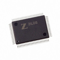
Z8018008FSG Zilog, Z8018008FSG Datasheet - Page 71

Z8018008FSG
Manufacturer Part Number
Z8018008FSG
Description
IC 8MHZ Z180 CMOS ENH MPU 80-QFP
Manufacturer
Zilog
Datasheet
1.Z8018006PSG.pdf
(85 pages)
Specifications of Z8018008FSG
Processor Type
Z180
Features
8-Bit, Enhanced Z80 Megacell
Speed
8MHz
Voltage
5V
Mounting Type
Surface Mount
Package / Case
80-BQFP
Processor Series
Z8018xx
Core
Z80
Data Bus Width
8 bit
Maximum Clock Frequency
8 MHz
Number Of Timers
2
Operating Supply Voltage
0 V to 5 V
Maximum Operating Temperature
+ 70 C
Mounting Style
SMD/SMT
Minimum Operating Temperature
0 C
Lead Free Status / RoHS Status
Lead free / RoHS Compliant
Other names
269-3882
Z8018008FSG
Z8018008FSG
Available stocks
Company
Part Number
Manufacturer
Quantity
Price
DMA/WAIT Control Register (DCNTL)
DMA/WAIT Control Register (DCNTL: I/O Address = 32h)
PS014004-1106
Bit
MMOD: Memory Mode Channel 0 (bit 1). When channel 0 is configured for memory
to/from memory transfers there is no
timing. Instead, two automatic transfer timing modes are selectable: burst (
cycle steal (
control of the bus continuously until the DMA transfer completes (the byte count register is
0
until the transfer is completed.
For channel 0 DMA with I/O source or destination, the selected
signal times the transfer and
DCNTL
I/O. DCNTL also defines the Request signal for each channel as level or edge sense.
also sets the DMA transfer mode for channel 1, which is limited to memory to/from I/O
transfers.
MWI1, MWI0: Memory Wait Insertion (bits 7-6)—Specifies the number of wait states
introduced into CPU or DMAC memory access cycles.
RESET
IWI1, IWI0: I/O Wait Insertion (bits 5-4)—Specifies the number of wait states
introduced into CPU or DMAC I/O access cycles.
DMS1, DMS0: DMA Request Sense (bits 3-2)—
request sense for channel 0 and channel 1 respectively. When reset to
sense. When set to
RESET
Typically, for an input/source device, the associated DMS bit must be
programmed as
update its
machine cycles involved in transferring a byte.
An output/destination device takes much less time to update its
DMA channel starts a
). In
MWI1
R/W
Figure 67. DMA/WAIT Control Register (DCNTL: I/O Address = 32h
7
CYCLE STEAL
.
.
controls the insertion of wait states into DMAC (and CPU) accesses of memory or
MWI0
R/W
REQUEST
6
MMOD = 0
0
for level sense because the device undertakes a relatively long period to
IWI1
R/W
1
5
, the input is edge sense.
signal after the DMA channel reads data from it in the first of the two
mode, the CPU is provided a cycle for each DMA byte transfer cycle
WRITE
). For burst memory to/from memory transfers, the DMAC takes
R/W
IWI0
4
MMOD
operation to it, as the
DMS1
R/W
3
is ignored.
REQUEST HANDSHAKE
DMS0
R/W
2
DMS1
MMOD
IWI1
DIM1
R/W
and
1
DMS1
MWI1
is cleared to
and
DMS0
DIM0
R/W
IWI0
0
and
and
signal to control the transfer
are cleared to
REQUEST
REQUEST HANDSHAKE
are set to
DMS0
MWI0
Microprocessor Unit
0
0
during
, the input is level
specify the DMA
are set to
signal, after the
MMOD = 1
1
during
0
RESET
during
Architecture
1
Z80180
DCNTL
.
RESET
during
) and
.
65


