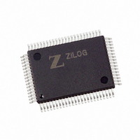
Z8018008FSG Zilog, Z8018008FSG Datasheet - Page 17

Z8018008FSG
Manufacturer Part Number
Z8018008FSG
Description
IC 8MHZ Z180 CMOS ENH MPU 80-QFP
Manufacturer
Zilog
Datasheet
1.Z8018006PSG.pdf
(85 pages)
Specifications of Z8018008FSG
Processor Type
Z180
Features
8-Bit, Enhanced Z80 Megacell
Speed
8MHz
Voltage
5V
Mounting Type
Surface Mount
Package / Case
80-BQFP
Processor Series
Z8018xx
Core
Z80
Data Bus Width
8 bit
Maximum Clock Frequency
8 MHz
Number Of Timers
2
Operating Supply Voltage
0 V to 5 V
Maximum Operating Temperature
+ 70 C
Mounting Style
SMD/SMT
Minimum Operating Temperature
0 C
Lead Free Status / RoHS Status
Lead free / RoHS Compliant
Other names
269-3882
Z8018008FSG
Z8018008FSG
Available stocks
Company
Part Number
Manufacturer
Quantity
Price
PS014004-1106
RXS—
CSIO
ST—
decode the status of the CPU machine cycle.
Table 3. Status Summary
TEND0, TEND1—
during the most recent
operation. It is used to indicate the end of the block transfer.
CKA1
TEST—
TOUT—
line is multiplexed with A18 of the address bus.
TXA0, TXA1—
ted data from the ASCI channels. Transmitted data changes are with respect to the falling
edge of the transmit clock.
TXS—
from the CSIO channel.
WAIT—
I/O devices are not ready for a data transfer. This input is sampled on the falling edge of T2
(and subsequent wait states). If the input is sampled Low, then the additional wait states are
inserted until the
WR—WRITE
data to be stored at the addressed I/O or memory location.
XTAL—
open if an external clock is used instead of a crystal. The oscillator input is not a
ST
0
1
1
0
0
1
Notes:
X = Reserved.
MC = Machine Cycle.
Status (output, active High). This signal is used with the
channel.
.
Clocked Serial Transmit Data (output, active High). This line is the transmitted data
Clocked Serial Receive Data (input, active High). This line is the receiver data for the
Test (output, not in DIP version). This pin is for test and must be left open.
Wait (input, active Low).
Crystal (input, active High). Crystal oscillator connection. This pin must be left
Timer Out (output, active High).
HALT
1
1
1
X
0
0
(output, active Low, 3-state).
RXS
Transmit Data 0 and 1 (outputs, active High). These signals are the transmit-
WAIT
Transfer End 0 and 1 (outputs, active Low). This output is asserted active
M1
0
0
1
1
0
1
is multiplexed with the
WRITE
input is sampled high, at which time execution continues.
Operation
CPU Operation (1st opcode fetch)
CPU Operation (2nd opcode and 3rd opcode
fetch)
CPU Operation (MC except for opcode fetch)
DMA Operation
HALT Mode
SLEEP Mode (including SYSTEM STOP
Mode)
cycle of a DMA
WAIT
indicated to the MPU that the addressed memory or
T
OUT
WR
CTS1
is the pulse output from PRT channel 1. This
indicated that the CPU data bus holds valid
signal for ASCI channel 1.
TEND0
M1
and
Microprocessor Unit
is multiplexed with
HALT
output to
TTL
Overview
Z80180
level
11


