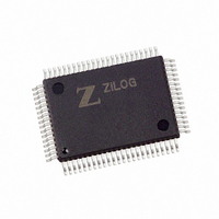
Z8018008FSG Zilog, Z8018008FSG Datasheet - Page 50

Z8018008FSG
Manufacturer Part Number
Z8018008FSG
Description
IC 8MHZ Z180 CMOS ENH MPU 80-QFP
Manufacturer
Zilog
Datasheet
1.Z8018006PSG.pdf
(85 pages)
Specifications of Z8018008FSG
Processor Type
Z180
Features
8-Bit, Enhanced Z80 Megacell
Speed
8MHz
Voltage
5V
Mounting Type
Surface Mount
Package / Case
80-BQFP
Processor Series
Z8018xx
Core
Z80
Data Bus Width
8 bit
Maximum Clock Frequency
8 MHz
Number Of Timers
2
Operating Supply Voltage
0 V to 5 V
Maximum Operating Temperature
+ 70 C
Mounting Style
SMD/SMT
Minimum Operating Temperature
0 C
Lead Free Status / RoHS Status
Lead free / RoHS Compliant
Other names
269-3882
Z8018008FSG
Z8018008FSG
Available stocks
Company
Part Number
Manufacturer
Quantity
Price
PS014004-1106
of
Configuration Register is
is inhibited (forced to
If the
then writing to this bit sets the prescale (PS) control. Under these circumstances, a
cates a divide-by-10 prescale function, while a
PEO: Parity Even Odd (bit 4)—
enabling/disabling of parity (
selected. If
DR: Divide Ratio (bit 3)—If the
divider used to obtain baud rate from the data sampling clock. If
16 is used, while if
SS2,1,0: Source/Speed Select 2,1,0 (bits 2–0)—If these bits are
RESET
DR
If these bits are not
two divider for the
Setting or leaving these bits as
selected for the
System Configuration Register is
the Interrupt Edge register is
Table 12. Divide Ratio
SS2
0
0
0
0
1
1
1
1
CNTLB0
bit and the
SS2–0
, the
SS1
0
0
1
1
0
0
1
1
PEO
in a real-time, positive-logic fashion (
CKA
bits in this register are not
X1
CKA
is set to
pin is used as a clock input, and is divided by 1, 16, or 64 depending on the
SS0
0
1
0
1
0
1
0
1
bit in the
PHI
DR
111
function.
0
). Bit
is set to
clock as indicated in
and the
1
0
, odd parity is selected.
Divide Ratio
÷1
÷2
÷4
÷8
÷16
÷32
÷64
External Clock
to auto-enable
ASEXT
5
MOD1
1
.
of
CKAO/CKS
111
1
BRG
, divide-by-64 is used.
CNTLB1
0
makes sense for a channel only when its
.
X1
register.
PEO
bit of
DCD0/CKA1
mode bit is
111
bit in the
selects oven or odd parity.
, and the
CTS0
CNTLA
reads back as
features the
Table
1
, and the pin is negated (High), the
ASEXT
ASEXT
indicates divide-by-30. The bit resets to
HIGH = 1
features the
PEO
). If
BRG
12.
PEO
is cleared to
CKAO
DR
mode bit in the
register is
is
0
.
,
0
is cleared to
is cleared to
LOW
, these bits specify a power-of-
CKA1
function when bit
DR
= 0). If bit
0
0
PEO
Microprocessor Unit
, this bit specifies the
function when bit
is reset to
during
111
ASEXT
0
0
does not affect the
, even parity is
during
, as they are after
CKA
RESET
5
in the System
0
register is
, divide- by-
Architecture
4
RESET
pin is
of the
TDRE
0
.
Z80180
indi-
0
.
of
bit
0
0
.
,
44


