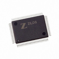
Z8018008FSG Zilog, Z8018008FSG Datasheet - Page 57

Z8018008FSG
Manufacturer Part Number
Z8018008FSG
Description
IC 8MHZ Z180 CMOS ENH MPU 80-QFP
Manufacturer
Zilog
Datasheet
1.Z8018006PSG.pdf
(85 pages)
Specifications of Z8018008FSG
Processor Type
Z180
Features
8-Bit, Enhanced Z80 Megacell
Speed
8MHz
Voltage
5V
Mounting Type
Surface Mount
Package / Case
80-BQFP
Processor Series
Z8018xx
Core
Z80
Data Bus Width
8 bit
Maximum Clock Frequency
8 MHz
Number Of Timers
2
Operating Supply Voltage
0 V to 5 V
Maximum Operating Temperature
+ 70 C
Mounting Style
SMD/SMT
Minimum Operating Temperature
0 C
Lead Free Status / RoHS Status
Lead free / RoHS Compliant
Other names
269-3882
Z8018008FSG
Z8018008FSG
Available stocks
Company
Part Number
Manufacturer
Quantity
Price
ASCI Extension Control Registers, Channel 0 and 1
PS014004-1106
Bit
Bit
Reserved
Reserved Reserved Reserved
DCD0 dis (bit 6, ASCI0 only)—If bit
DCD0
ASCI0
of the
In either state of this bit, software can read the state of the
and the receiver interrupts on a rising edge of
CTS0 dis (bit 5, ASCI0 only)—If bit
select the
enables the
STAT0
1
this bit, software can read the state of the
X1 (bit 4)—If this bit is
as a 1X bit clock (sometimes called isochronous mode). In this mode, receive data on the
RXA
input or an output. If this bit is
divided by 16 or 64 per the
mode, receive data on the
BRG Mode (bit 3)—If the
the ASCI Baud Rate Generator divides
and then by a power of two selected by the
the transmitter and receiver and that can be output on the
this bit is
into the Time Constant Registers, plus 2). This mode is identical to the operation of the baud
rate generator in the ESCC.
Break Enable (bit 2)—If this bit is
them in bit
, the state of the
7
7
Figure 42. ASCI Extension Control Registers, Channel 0 and 1
pin must be synchronized to the clock on the
IER
function for the
receiver. When the pin is negated/High, the Receiver is held in a
ASCI Extension Control Register 0(ASEXT0 I/O Address = 12h)
register is forced to
ASCI Extension Control Register 1 (ASEXT1 I/O Address = 13h)
DCDO
1
CTS0
is
, the Baud Rate Generator divides
6
6
1
ASCIO
, and the transmitter sends breaks under the control of bit
0
and this bit is
function of the
CTSO
CTS0
transmitter, in that when the pin is negated (High), the
5
5
DCD0
pin exhibits no effect on the transmitter. Regardless of the state of
1
RXA
, the clock from the Baud Rate Generator or
0
XI
XI
4
4
DR
. If bit
/
1
SS2–0
CKA1
, the state of the
CTS0
0
bit in
pin is not required to be synchronized to a clock.
, the clock from the Baud Rate Generator or
BRGO
Mode
BRGI
Mode
5
bits in the
3
3
pin, and this bit is
/
of the System Configuration Register is
RXS
CNTLB
1
, the receiver detects break conditions and report
PHI
5
0
CTS0
pin, and this bit is
Nab
Enab
Break
Break
of the System Configuration Register is
SS2–0
of the Interrupt Edge Register is
by 10 or 30, depending on the
2
2
register, to obtain the actual bit rate. In this
PHI
CNTLB
DCD0
DCD
pin the
bits, to obtain the clock that is presented to
by twice (the 16-bit value programmed
CKA
Break
Break
-pin has no effect on receiver operation.
.
1
1
register are not
0
CNTLB0
pin, regardless of whether
, the
CKA
DCD0
Send
Break
Send
Break
DCD0
0
0
0
, then the
pin. If
register.
pin in the
pin auto-enables the
Microprocessor Unit
111
SS2–0
0
CKA
.
RESET
CTS0
, and this bit is
TDRE
DR
STAT0
0
are not
pin is received
0
CKA
to select the
pin auto-
bit in
and this bit is
state. If bit
Architecture
bit in the
CKA
pin is
register,
0
CNTLB
111
Z80180
to
, and
is an
0
,
0
,
51


