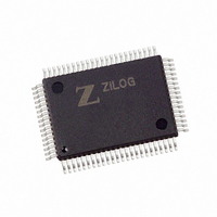
Z8018008FSG Zilog, Z8018008FSG Datasheet - Page 16

Z8018008FSG
Manufacturer Part Number
Z8018008FSG
Description
IC 8MHZ Z180 CMOS ENH MPU 80-QFP
Manufacturer
Zilog
Datasheet
1.Z8018006PSG.pdf
(85 pages)
Specifications of Z8018008FSG
Processor Type
Z180
Features
8-Bit, Enhanced Z80 Megacell
Speed
8MHz
Voltage
5V
Mounting Type
Surface Mount
Package / Case
80-BQFP
Processor Series
Z8018xx
Core
Z80
Data Bus Width
8 bit
Maximum Clock Frequency
8 MHz
Number Of Timers
2
Operating Supply Voltage
0 V to 5 V
Maximum Operating Temperature
+ 70 C
Mounting Style
SMD/SMT
Minimum Operating Temperature
0 C
Lead Free Status / RoHS Status
Lead free / RoHS Compliant
Other names
269-3882
Z8018008FSG
Z8018008FSG
Available stocks
Company
Part Number
Manufacturer
Quantity
Price
PS014004-1106
interrupt before operation resumes. It is also used with the
status of the CPU machine cycle.
INT0
nal I/O devices. The CPU honors these requests at the end of the current instruction cycle as
long as the
signals are inactive. The CPU acknowledges this interrupt request with an interrupt
acknowledge cycle. During this cycle, both the
INT1
ated by external I/O devices. The CPU honors these requests at the end of the current
instruction cycle as long as the
acknowledges these requests with an interrupt acknowledge cycle. Unlike the acknowledg-
ment for
IORQ
tains a valid I/O address for an I/O
along with
rupt response vector can be placed onto the data bus. This signal is analogous to the
nal of the Z64180.
M1
rent cycle is the opcode fetch cycle of and instruction execution. Together with
indicates that the current cycle is for an interrupt acknowledge. It is also used with the
and
signal of the Z64180.
MREQ
bus holds a valid address for a memory
analogous to the
NMI
ity than
the interrupt enable flip-flops. This signal forces CPU execution to continue at location
0066h
RD
read data from memory or an I/O device. The addressed I/O or memory device must use this
signal to gate data onto the CPU data bus.
RFSH
CPU machine cycle and the contents of the address bus must be used for refresh of dynamic
memories. The low order 8 bits of the address bus (
This signal is analogous to the
RTS0
ASCI channel 0.
RXA0, RXA1—
to the ASCI channels.
—Machine Cycle 1 (output, active Low). Together with
—Opcode Reinitialized (output, active Low, 3-state).
ST
—Nonmaskable Interrupt (input, negative edge triggered).
—Maskable Interrupt Request 0 (input, active Low). This signal is generated by exter-
,
.
—I/O Request (output, active Low, 3-state).
—Request to Send 0 (output, active Low). A programmable modem control signal for
—Refresh (output, active Low). Together with
INT2
—Memory Request (output, active Low, 3-state).
signal to decode status of the CPU machine cycle. This signal is analogous to the
INT
INT0
M1
—Maskable Interrupt Request 1 and 2 (inputs, active Low). This signal is gener-
NMI
and is always recognized at the end of an instruction, regardless of the state of
, during this cycle neither the
, during the acknowledgment of the
Receive Data 0 and 1 (input, active High). These signals are the receive data
and
ME
BUSREQ
signal of Z64180.
REF
NMI
READ
,
signal of the Z64180.
BUSREQ
READ
or I/O
M1
, and
or memory
M1
or
WRITE
IORQ
IORQ
INT0
and
A7–A10
INT0
MREQ
IORQ
input signal to indicate that an inter-
signals become active.
indicates that the address bus con-
operation.
RD
MREQ
signals are inactive. The CPU
WRITE
M1
MREQ
) contain the refresh address.
,
indicated that the CPU wants to
RFSH
signals become active.
and
NMI
indicates that the address
,
operation. This signal is
ST
M1
indicates that the current
IORQ
Microprocessor Unit
demands a higher prior-
signals to decode
indicates that the cur-
is also generated,
IORQ
Overview
Z80180
IOE
,
HALT
M1
LIR
sig-
10


