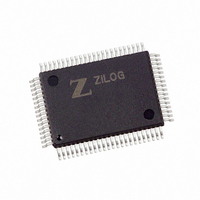
Z8018008FSG Zilog, Z8018008FSG Datasheet - Page 72

Z8018008FSG
Manufacturer Part Number
Z8018008FSG
Description
IC 8MHZ Z180 CMOS ENH MPU 80-QFP
Manufacturer
Zilog
Datasheet
1.Z8018006PSG.pdf
(85 pages)
Specifications of Z8018008FSG
Processor Type
Z180
Features
8-Bit, Enhanced Z80 Megacell
Speed
8MHz
Voltage
5V
Mounting Type
Surface Mount
Package / Case
80-BQFP
Processor Series
Z8018xx
Core
Z80
Data Bus Width
8 bit
Maximum Clock Frequency
8 MHz
Number Of Timers
2
Operating Supply Voltage
0 V to 5 V
Maximum Operating Temperature
+ 70 C
Mounting Style
SMD/SMT
Minimum Operating Temperature
0 C
Lead Free Status / RoHS Status
Lead free / RoHS Compliant
Other names
269-3882
Z8018008FSG
Z8018008FSG
Available stocks
Company
Part Number
Manufacturer
Quantity
Price
Interrupt Vector Low Register
Interrupt Vector Low Register (IL: I/O Address = 33h)
PS014004-1106
Bit
second machine cycle of the two cycles involved in transferring a byte. With zero-wait state
I/O cycles, which apply only to the ASCIs, it is impossible for a device to update its
REQUEST
With one-wait-state I/O cycles (the fastest possible except for the ASCIs), it is unlikely that
an output device is able to update its
to the ESCC and bidirectional Centronics controller, and is recommended for external output
devices connected to
With two or more wait states in I/O cycles, external output devices on
edge or level sense depending on their characteristics; edge sense is still recommended for
output on the ESCC and bidirectional Centronics controller.
DIM1, DIM0: DMA Channel 1 I/O and Memory Mode (bits 1-0)—Specifies the
source/destination and address modifier for channel 1 memory to/from I/O transfer modes.
DIM1
Table 18. Channel 1 Transfer Mode
Mnemonic: IL
Address 33
Bits
INT1
to
DIM1 DMI0 Transfer Mode Address Increment/Decrement
0
0
1
1
R/W
IL 7
0
7
Programmable
Figure 68. Interrupt Vector Low Register (IL: I/O Address = 33h)
during
7–5
and
and
0
1
0
1
of
R/W
IL 6
INT2
6
DIM0
signal in time, and edge sensing must be used.
IL
RESET
are used as bits
Memory→I/O
Memory→I/O
I/O→Memory
I/O→Memory
pins and for the DMAs, ASCIs,
R/W
are cleared to
IL 5
5
(Figure
T
OUT
––
4
Interrupt Source Dependent Code
/
68).
DREQ
7–5
0
––
3
during
MAR1 +1, IAR1 fixed
MAR1–1, IAR1 fixed
IAR1 fixed, MAR1 + 1
IAR1 fixed, MAR1 –1
.
of the synthesized interrupt vector during interrupts for the
REQUEST
––
RESET
2
.
––
in time, and edge sense is required for output
1
PRTs
, and
––
0
CSIO
. These three bits are cleared
Microprocessor Unit
T
OUT
/
DREQ
Architecture
can use
Z80180
66


