MK60DX256ZVLL10 Freescale Semiconductor, MK60DX256ZVLL10 Datasheet - Page 13
MK60DX256ZVLL10
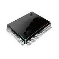
Manufacturer Part Number
MK60DX256ZVLL10
Description
KINETIS 256KFLEX ENET
Manufacturer
Freescale Semiconductor
Specifications of MK60DX256ZVLL10
Processor Series
K60
Core
ARM Cortex M4
Data Bus Width
16 bit
Program Memory Type
Flash
Program Memory Size
256 KB
Data Ram Size
128 KB
Interface Type
USB, CAN, SPI, I2C, UART
Maximum Clock Frequency
100 MHz
Number Of Programmable I/os
2
Number Of Timers
2
Operating Supply Voltage
1.71 V to 3.6 V
Maximum Operating Temperature
+ 105 C
Mounting Style
SMD/SMT
Package / Case
LQFP-100
Operating Temperature Range
- 40 C to + 105 C
Processor To Be Evaluated
MK60DX256ZVLL10
Supply Current (max)
185 mA
Lead Free Status / Rohs Status
Details
Available stocks
Company
Part Number
Manufacturer
Quantity
Price
Company:

Part Number:
MK60DX256ZVLL10
Manufacturer:
Freescale Semiconductor
Quantity:
10 000


1. All 5 volt tolerant digital I/O pins are internally clamped to V
2. Analog pins are defined as pins that do not have an associated general purpose I/O port function.
3. All analog pins are internally clamped to V
5.1.2 LVD and POR operating requirements
Freescale Semiconductor, Inc.
Symbol
V
V
V
V
V
Symbol
V
V
V
connection to V
resistors at the pads. If this limit cannot be observed then a current limiting resistor is required. The negative DC injection
current limiting resistor is calculated as R=(V
(=V
resistors at the pads. If these limits cannot be observed then a current limiting resistor is required. The negative DC
injection current limiting resistor is calculated as R=(V
calcualted as R=(V
V
I
LVW1H
LVW2H
LVW3H
LVW4H
I
V
RFVBAT
HYSH
ICcont
LVDH
ICAIO
LVDL
POR
RAM
SS
-0.3V) and V
Falling VDD POR detect voltage
Falling low-voltage detect threshold — high
range (LVDV=01)
Low-voltage warning thresholds — high range
Low-voltage inhibit reset/recover hysteresis —
high range
Falling low-voltage detect threshold — low range
(LVDV=00)
Description
Analog
— single pin
Contiguous pin DC injection current —regional limit,
includes sum of negative injection currents or sum of
positive injection currents of 16 contiguous pins
V
V
Description
Table 1. Voltage and current operating requirements (continued)
DD
BAT
• Level 1 falling (LVWV=00)
• Level 2 falling (LVWV=01)
• Level 3 falling (LVWV=10)
• Level 4 falling (LVWV=11)
• V
• V
• Negative current injection
• Positive current injection
voltage required to retain RAM
DD
Table 2. V
voltage required to retain the VBAT register file
. If V
2
IN
IN
IN
, EXTAL, and XTAL pin DC injection current
IN
-V
< V
> V
is less than V
IN
AIO_MAX
SS
DD
greater than V
-0.3V (Negative current injection)
+0.3V (Positive current injection)
K60 Sub-Family Data Sheet Data Sheet, Rev. 5, 5/2011.
)/|I
DD
IC
AIO_MAX
|. Select the larger of these two calculated resistances.
supply LVD and POR operating requirements
DIO_MIN
Table continues on the next page...
(=V
SS
DIO_MIN
and V
DD
(=V
+0.3V) is observed, then there is no need to provide current limiting
SS
DD
-V
Preliminary
-0.3V) is observed, then there is no need to provide current limiting
AIO_MIN
IN
through ESD protection diodes. If V
)/|I
IC
SS
|.
-V
through a ESD protection diode. There is no diode
IN
TBD
TBD
TBD
TBD
TBD
TBD
TBD
Min.
)/|I
IC
|. The positive injection current limiting resistor is
TBD
Min.
-25
1.2
-5
—
—
2.56
2.70
2.80
2.90
3.00
1.60
Typ.
1.1
60
Max.
+25
+5
—
—
—
—
Max.
TBD
TBD
TBD
TBD
TBD
TBD
TBD
IN
is greater than V
Unit
mA
mA
V
V
Unit
mV
V
V
V
V
V
V
V
AIO_MIN
Notes
Notes
General
3
1
13
Related parts for MK60DX256ZVLL10
Image
Part Number
Description
Manufacturer
Datasheet
Request
R

Part Number:
Description:
Manufacturer:
Freescale Semiconductor, Inc
Datasheet:
Part Number:
Description:
Manufacturer:
Freescale Semiconductor, Inc
Datasheet:
Part Number:
Description:
Manufacturer:
Freescale Semiconductor, Inc
Datasheet:
Part Number:
Description:
Manufacturer:
Freescale Semiconductor, Inc
Datasheet:
Part Number:
Description:
Manufacturer:
Freescale Semiconductor, Inc
Datasheet:
Part Number:
Description:
Manufacturer:
Freescale Semiconductor, Inc
Datasheet:
Part Number:
Description:
Manufacturer:
Freescale Semiconductor, Inc
Datasheet:
Part Number:
Description:
Manufacturer:
Freescale Semiconductor, Inc
Datasheet:
Part Number:
Description:
Manufacturer:
Freescale Semiconductor, Inc
Datasheet:
Part Number:
Description:
Manufacturer:
Freescale Semiconductor, Inc
Datasheet:
Part Number:
Description:
Manufacturer:
Freescale Semiconductor, Inc
Datasheet:
Part Number:
Description:
Manufacturer:
Freescale Semiconductor, Inc
Datasheet:
Part Number:
Description:
Manufacturer:
Freescale Semiconductor, Inc
Datasheet:
Part Number:
Description:
Manufacturer:
Freescale Semiconductor, Inc
Datasheet:
Part Number:
Description:
Manufacturer:
Freescale Semiconductor, Inc
Datasheet: