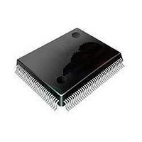
MK60DX256ZVLL10 Freescale Semiconductor, MK60DX256ZVLL10 Datasheet - Page 65

MK60DX256ZVLL10
Manufacturer Part Number
MK60DX256ZVLL10
Description
KINETIS 256KFLEX ENET
Manufacturer
Freescale Semiconductor
Specifications of MK60DX256ZVLL10
Processor Series
K60
Core
ARM Cortex M4
Data Bus Width
16 bit
Program Memory Type
Flash
Program Memory Size
256 KB
Data Ram Size
128 KB
Interface Type
USB, CAN, SPI, I2C, UART
Maximum Clock Frequency
100 MHz
Number Of Programmable I/os
2
Number Of Timers
2
Operating Supply Voltage
1.71 V to 3.6 V
Maximum Operating Temperature
+ 105 C
Mounting Style
SMD/SMT
Package / Case
LQFP-100
Operating Temperature Range
- 40 C to + 105 C
Processor To Be Evaluated
MK60DX256ZVLL10
Supply Current (max)
185 mA
Lead Free Status / Rohs Status
Details
Available stocks
Company
Part Number
Manufacturer
Quantity
Price
Company:
Part Number:
MK60DX256ZVLL10
Manufacturer:
Freescale Semiconductor
Quantity:
10 000
6.8.11 I
This section provides the AC timings for the I
modes (clocks input). All timings are given for non-inverted serial clock polarity
(TCR[TSCKP] = 0, RCR[RSCKP] = 0) and a non-inverted frame sync (TCR[TFSI] = 0,
RCR[RFSI] = 0). If the polarity of the clock and/or the frame sync have been inverted, all
the timings remain valid by inverting the clock signal (I2S_BCLK) and/or the frame sync
(I2S_FS) shown in the figures below.
Freescale Semiconductor, Inc.
I2S_MCLK (output)
I2S_BCLK (output)
I2S_FS (output)
I2S_FS (input)
I2S_TXD
I2S_RXD
Num
S10
S1
S2
S3
S4
S5
S6
S7
S8
S9
2
S switching specifications
Operating voltage
I2S_MCLK cycle time
I2S_MCLK pulse width high/low
I2S_BCLK cycle time
I2S_BCLK pulse width high/low
I2S_BCLK to I2S_FS output valid
I2S_BCLK to I2S_FS output invalid
I2S_BCLK to I2S_TXD valid
I2S_BCLK to I2S_TXD invalid
I2S_RXD/I2S_FS input setup before I2S_BCLK
I2S_RXD/I2S_FS input hold after I2S_BCLK
Description
S5
S7
K60 Sub-Family Data Sheet Data Sheet, Rev. 5, 5/2011.
S4
Figure 29. I
Table 47. I
S9
S9
S1
S3
S2
S10
2
S timing — master mode
2
S master mode timing
Preliminary
S4
S2
2
S in master (clocks driven) and slave
S8
S7
Peripheral operating requirements and behaviors
2 x t
5 x t
45%
45%
Min.
-2.5
2.7
20
—
—
-3
0
SYS
SYS
Max.
55%
55%
3.6
15
15
—
—
—
—
—
MCLK period
S10
BCLK period
S6
S8
Unit
ns
ns
ns
ns
ns
ns
ns
ns
V
65


