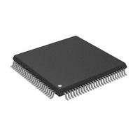
AD9882AKSTZ-100 Analog Devices Inc, AD9882AKSTZ-100 Datasheet - Page 10

AD9882AKSTZ-100
Manufacturer Part Number
AD9882AKSTZ-100
Description
IC INTERFACE/DVI 100MHZ 100LQFP
Manufacturer
Analog Devices Inc
Datasheet
1.AD9882KSTZ-100.pdf
(40 pages)
Specifications of AD9882AKSTZ-100
Applications
Video
Interface
Analog, DVI
Voltage - Supply
3.15 V ~ 3.45 V
Package / Case
100-LQFP
Mounting Type
Surface Mount
Supply Voltage Range
3.15V To 3.45V, 2.2V To 3.45V
Operating Temperature Range
0°C To +70°C
Digital Ic Case Style
LQFP
No. Of Pins
100
Msl
MSL 3 - 168 Hours
Update Rate
140MSPS
Bandwidth
300MHz
Rohs Compliant
Yes
Lead Free Status / RoHS Status
Lead free / RoHS Compliant
Available stocks
Company
Part Number
Manufacturer
Quantity
Price
Company:
Part Number:
AD9882AKSTZ-100
Manufacturer:
AD
Quantity:
1 200
Company:
Part Number:
AD9882AKSTZ-100
Manufacturer:
ADI
Quantity:
352
Company:
Part Number:
AD9882AKSTZ-100
Manufacturer:
Analog Devices Inc
Quantity:
10 000
Part Number:
AD9882AKSTZ-100
Manufacturer:
ADI/亚德诺
Quantity:
20 000
AD9882A
FILT—External Filter Connection
For proper operation, the pixel clock generator PLL requires an
external filter. Connect the filter as shown in Figure 8 to this
pin. For optimal performance, minimize noise and parasitics on
this node.
REFBYPASS—Internal Reference Bypass
Bypass for the internal 1.25 V band gap reference. It should be
connected to ground through a 0.1 µF capacitor.
The absolute accuracy of this reference is ±4%, and the temp-
erature coefficient is ±50 ppm, which is adequate for most
AD9882A applications. If higher accuracy is required, an
external reference can be employed instead.
MIDBYPASS—Midscale Voltage Reference Bypass
Bypass for the internal midscale voltage reference. It should be
connected to ground through a 0.1 µF capacitor. The exact
voltage varies with the gain setting of the red channel.
HSOUT—Horizontal Sync Output
A reconstructed and phase-aligned version of the Hsync input.
The duration of Hsync can be programmed only on the analog
interface, not the digital.
DATACK—Data Output Clock
The data clock output signal is used to clock the output data
and HSOUT into external logic. It is produced by the internal
clock generator and is synchronous with the internal pixel
sampling clock.
When the sampling time is changed by adjusting the phase
register, the output timing is shifted as well. The data bits,
DATACK, and HSOUT outputs are all moved, so the timing
relationship among the signals is maintained.
VSOUT—Vertical Sync Output
The separated Vsync from a composite signal or a direct pass-
through of the Vsync input. The polarity of this output can be
controlled via Register 0x10, Bit 2. The placement and duration
in all modes is set by the graphics transmitter.
Rev. 0 | Page 10 of 40
RED—Data Output, Red Channel
GREEN—Data Output, Green Channel
BLUE—Data Output, Blue Channel
These are the main data outputs. Bit 7 is the MSB.
The delay from pixel sampling time to output is fixed. When the
sampling time is changed by adjusting the phase register, the
output timing is shifted as well. The DATACK and HSOUT
outputs are also moved, so the timing relationship among the
signals is maintained. See the Timing Diagrams section for
more information.
POWER SUPPLY
V
These pins supply power to the main elements of the circuit.
They should be as quiet as possible.
V
A large number of output pins (up to 25) switching at high
speed (up to 140 MHz) generates a lot of power supply transi-
ents. These supply pins are identified separately from the V
pins, so special care must be taken to minimize output noise
transferred into the sensitive analog circuitry.
If the AD9882A is interfacing with lower voltage logic, V
be connected to a lower supply voltage (as low as 2.2 V) for
compatibility.
PV
The most sensitive portion of the AD9882A is the clock gener-
ation circuitry. These pins provide power to the clock PLL and
help the user design for optimal performance. The designer
should provide noise-free power to these pins.
GND—Ground
The ground return for all circuitry on-chip. It is recommended
that the AD9882A be assembled on a single solid ground plane,
with careful attention to ground current paths.
D
DD
—Main Power Supply
D
—Digital Output Power Supply
—Clock Generator Power Supply
DD
D
can


