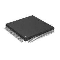
AD9882AKSTZ-100 Analog Devices Inc, AD9882AKSTZ-100 Datasheet - Page 13

AD9882AKSTZ-100
Manufacturer Part Number
AD9882AKSTZ-100
Description
IC INTERFACE/DVI 100MHZ 100LQFP
Manufacturer
Analog Devices Inc
Datasheet
1.AD9882KSTZ-100.pdf
(40 pages)
Specifications of AD9882AKSTZ-100
Applications
Video
Interface
Analog, DVI
Voltage - Supply
3.15 V ~ 3.45 V
Package / Case
100-LQFP
Mounting Type
Surface Mount
Supply Voltage Range
3.15V To 3.45V, 2.2V To 3.45V
Operating Temperature Range
0°C To +70°C
Digital Ic Case Style
LQFP
No. Of Pins
100
Msl
MSL 3 - 168 Hours
Update Rate
140MSPS
Bandwidth
300MHz
Rohs Compliant
Yes
Lead Free Status / RoHS Status
Lead free / RoHS Compliant
Available stocks
Company
Part Number
Manufacturer
Quantity
Price
Company:
Part Number:
AD9882AKSTZ-100
Manufacturer:
AD
Quantity:
1 200
Company:
Part Number:
AD9882AKSTZ-100
Manufacturer:
ADI
Quantity:
352
Company:
Part Number:
AD9882AKSTZ-100
Manufacturer:
Analog Devices Inc
Quantity:
10 000
Part Number:
AD9882AKSTZ-100
Manufacturer:
ADI/亚德诺
Quantity:
20 000
THEORY OF OPERATION AND DESIGN GUIDE: ANALOG INTERFACE
GENERAL DESCRIPTION
The AD9882A is a fully integrated solution for capturing analog
RGB signals and digitizing them for display on flat panel moni-
tors or projectors. The device is ideal for implementing a com-
puter interface for HDTV monitors or as the front end to high
performance video scan converters.
Implemented in a high performance CMOS process, the inter-
face can capture signals with pixel rates of up to 140 MHz.
The AD9882A includes all necessary input buffering, signal dc
restoration (clamping), offset and gain (brightness and contrast)
adjustment, pixel clock generation, sampling phase control, and
output data formatting. All controls are programmable via a
2-wire serial interface. Full integration of these sensitive analog
functions makes the system design straightforward and less
sensitive to the physical and electrical environment.
With a typical power dissipation of only 875 mW and an oper-
ating temperature range of 0°C to 70°C, the device requires no
special environmental considerations.
INPUT SIGNAL HANDLING
The AD9882A has three high impedance analog input pins for
the red, green, and blue channels. They will accommodate
signals ranging from 0.5 V to 1.0 V p-p.
Signals are typically brought onto the interface board via a
DVI-I connector, a 15-pin D connector, or BNC connectors.
The AD9882A should be located as close as practical to the
input connector. Signals should be routed via matched-
impedance traces (normally 75 Ω) to the IC input pins.
At that point, the signal should be resistively terminated (75 Ω
to the signal ground return) and capacitively coupled to the
AD9882A inputs through 47 nF capacitors. These capacitors
form part of the dc restoration circuit (see Figure 9).
In an ideal world of perfectly matched impedances, the best
performance can be obtained with the widest possible signal
bandwidth. The wide bandwidth inputs of the AD9882A
(300 MHz) can track the input signal continuously as it moves
from one pixel level to the next and digitize the pixel during a
long, flat pixel time. In many systems, however, there are
mismatches, reflections, and noise, which can result in excessive
ringing and distortion of the input waveform. This makes it
more difficult to establish a sampling phase that provides good
image quality. It has been shown that a small inductor in series
with the input is effective in rolling off the input bandwidth
slightly and providing a high quality signal over a wider range
of conditions. Using a Fair-Rite #2508051217Z0 high speed
signal chip bead inductor in the circuit of Figure 9 gives good
results in most applications.
Rev. 0 | Page 13 of 40
HSYNC AND VSYNC INPUTS
The AD9882A receives a horizontal sync signal and uses it to
generate the pixel clock and clamp timing. This can be either a
sync signal directly from the graphics source or a preprocessed
TTL or CMOS level signal.
The Hsync input includes a Schmitt trigger buffer and is
capable of handling signals with long rise times, with superior
noise immunity. In typical PC-based graphic systems, the sync
signals are simply TTL level drivers, feeding unshielded wires in
the monitor cable. As such, no termination is required.
SERIAL CONTROL PORT
The serial control port is designed for 3.3 V logic. If there are
5 V drivers on the bus, these pins should be protected with
150 Ω series resistors placed between the pull-up resistors and
the input pins.
OUTPUT SIGNAL HANDLING
The digital outputs are designed and specified to operate from a
3.3 V power supply (V
as 2.5 V for compatibility with other 2.5 V logic.
CLAMPING
RGB Clamping
To properly digitize the incoming signal, the dc offset of the
input must be adjusted to fit the range of the on-board ADCs.
Most graphics systems produce RGB signals with black at
ground and white at approximately 0.75 V. However, if sync
signals are embedded in the graphics, the sync tip is often at
ground, and black is at 300 mV; white will be approximately
1.0 V. Some common RGB line amplifier boxes use emitter-
follower buffers to split signals and increase drive capability.
This introduces a 700 mV dc offset to the signal, which is
removed by clamping for proper capture by the AD9882A.
The key to clamping is to identify a portion (time) of the signal
when the graphics system is known to be producing black.
Originating from CRT displays, the electron beam is blanked by
sending a black level during horizontal retrace to prevent
disturbing the image. Most graphics systems maintain this
format of sending a black level between active video lines.
INPUT
RGB
Figure 3. Analog Input Interface Circuit
DD
). They can also work with a V
75Ω
47nF
R
G
B
AIN
AIN
AIN
AD9882A
DD
as low


