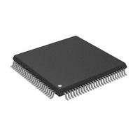
AD9882AKSTZ-100 Analog Devices Inc, AD9882AKSTZ-100 Datasheet - Page 31

AD9882AKSTZ-100
Manufacturer Part Number
AD9882AKSTZ-100
Description
IC INTERFACE/DVI 100MHZ 100LQFP
Manufacturer
Analog Devices Inc
Datasheet
1.AD9882KSTZ-100.pdf
(40 pages)
Specifications of AD9882AKSTZ-100
Applications
Video
Interface
Analog, DVI
Voltage - Supply
3.15 V ~ 3.45 V
Package / Case
100-LQFP
Mounting Type
Surface Mount
Supply Voltage Range
3.15V To 3.45V, 2.2V To 3.45V
Operating Temperature Range
0°C To +70°C
Digital Ic Case Style
LQFP
No. Of Pins
100
Msl
MSL 3 - 168 Hours
Update Rate
140MSPS
Bandwidth
300MHz
Rohs Compliant
Yes
Lead Free Status / RoHS Status
Lead free / RoHS Compliant
Available stocks
Company
Part Number
Manufacturer
Quantity
Price
Company:
Part Number:
AD9882AKSTZ-100
Manufacturer:
AD
Quantity:
1 200
Company:
Part Number:
AD9882AKSTZ-100
Manufacturer:
ADI
Quantity:
352
Company:
Part Number:
AD9882AKSTZ-100
Manufacturer:
Analog Devices Inc
Quantity:
10 000
Part Number:
AD9882AKSTZ-100
Manufacturer:
ADI/亚德诺
Quantity:
20 000
0x14 0
This bit configures the output data in 4:2:2 mode. This mode
can be used to reduce the number of data lines used from 24 to
16 for applications using YPbPr graphics signals. A timing
diagram for this mode is shown in Figure 17. Recommended
input and output configurations are shown in Table 39. In
4:2:2 mode, the red and blue channels can be interchanged to
help satisfy board layout or timing requirements, but the green
channel must be configured for Y.
Table 38. 4:2:2 Output Mode Select
Select
0
1
Table 39. 4:2:2 Input/Output Configuration
Channel
Red
Green
Blue
0x15 7
This bit is used to indicate when activity is detected on the
HSYNC input pin (Pin 79). If Hsync is held high or low, activity
is not detected.
Table 40. Hsync Detection Results
Detect
0
1
Figure 20 shows where this function is implemented.
0x15 6
This bit is used to indicate when sync activity is detected on the
sync-on-green input pin (Pin 64).
Table 41. Sync-on-Green Detection Results
Detect
0
1
Figure 20 shows where this function is implemented.
Note that if no sync signal is presented on the green video
input, normal video might still trigger activity.
0x15 5
This bit is used to indicate when activity is detected on the
Vsync input pin (Pin 80). If Vsync is held high or low, activity is
not detected.
Table 42. Vsync Detection Results
Detect
0
1
Figure 20 shows where this function is implemented.
4:2:2 Output Mode Select
Hsync Detect
Sync-on-Green Detect
Vsync Detect
Input Connection
Pr
Y
Pr
Function
No activity detected
Activity detected
Function
No activity detected
Activity detected
Function
No activity detected
Activity detected
Output Mode
4:4:4
4:2:2
Output Format
Pb/Pr
Y
High impedance
Rev. 0 | Page 31 of 40
0x15 4
This bit is used to indicate when activity is detected on the
digital interface clock input.
Table 43. Digital Interface Clock Detection Results
Detect
0
1
Figure 20 shows where this function is implemented.
0x15 3
This bit is used to indicate which interface should be active,
analog or digital. It checks for activity on the analog interface
and for activity on the digital interface, then determines which
should be active according to Table 44. Specifically, analog
interface detection is determined by OR’ing Bits 7, 6, and 5 in
this register. Digital interface detection is determined by Bit 4 in
this register. If both interfaces are detected, the user can
determine which has priority via Bit 1 in Register 0x0F. The
user can override this function via Bit 2 in Register 0x0F. If the
override bit is set to Logic 1, then this bit will be forced to the
same state as Bit 1 in Register 0x0F.
Table 44. Active Interface Results
Bits 7, 6, or 5
(Analog
Detection)
0
0
1
1
X
AI = 0 means analog interface. AI = 1 means digital interface.
The override bit is in Register 0x0F, Bit 2.
0x16 7
This bit indicates which Hsync input source is being used by
the PLL (Hsync input or sync-on-green). Bits 6 and 7 in
Register 0x15 determine which source is used. If both Hsync
and SOG are detected, the user can determine which has
priority via Bit 3 in Register 0x10. The user can override this
function via Bit 4 in Register 0x10. If the override bit is set to
Logic 1, then this bit will be forced to the same state as Bit 3 in
Register 0x10.
Digital Interface Clock Detect
Active Interface
AHS Active Hsync
Bit 4
(Digital
Detection)
0
1
0
1
X
Function
No activity detected
Activity detected
Override
0
0
0
0
1
AI
Soft power-
down (seek
mode)
1
0
Bit 1 in 0x0F
Bit 1 in 0x0F
AD9882A


