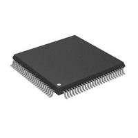
AD9882AKSTZ-100 Analog Devices Inc, AD9882AKSTZ-100 Datasheet - Page 29

AD9882AKSTZ-100
Manufacturer Part Number
AD9882AKSTZ-100
Description
IC INTERFACE/DVI 100MHZ 100LQFP
Manufacturer
Analog Devices Inc
Datasheet
1.AD9882KSTZ-100.pdf
(40 pages)
Specifications of AD9882AKSTZ-100
Applications
Video
Interface
Analog, DVI
Voltage - Supply
3.15 V ~ 3.45 V
Package / Case
100-LQFP
Mounting Type
Surface Mount
Supply Voltage Range
3.15V To 3.45V, 2.2V To 3.45V
Operating Temperature Range
0°C To +70°C
Digital Ic Case Style
LQFP
No. Of Pins
100
Msl
MSL 3 - 168 Hours
Update Rate
140MSPS
Bandwidth
300MHz
Rohs Compliant
Yes
Lead Free Status / RoHS Status
Lead free / RoHS Compliant
Available stocks
Company
Part Number
Manufacturer
Quantity
Price
Company:
Part Number:
AD9882AKSTZ-100
Manufacturer:
AD
Quantity:
1 200
Company:
Part Number:
AD9882AKSTZ-100
Manufacturer:
ADI
Quantity:
352
Company:
Part Number:
AD9882AKSTZ-100
Manufacturer:
Analog Devices Inc
Quantity:
10 000
Part Number:
AD9882AKSTZ-100
Manufacturer:
ADI/亚德诺
Quantity:
20 000
Table 23. Active Vsync Override Settings
Override
0
1
The default for this register is 0.
0x10 0
This bit is used to select the active Vsync when the override bit
is set (Bit 1).
Table 24. Active Vsync Select Settings
Select
0
1
The default for this register is 0.
0x11 7
This bit enables/disables clamping.
Table 25. Clamp Input Signal Source Settings
Clamp Function
0
1
0 enables the clamp timing circuitry controlled by clamp
placement and clamp duration. The clamp position and
duration is counted from the trailing edge of Hsync.
1 disables clamping. The three channels are clamped when the
clamp signal is active.
Power-up default value for clamp function is 0.
0x11 6
A bit that determines whether the red channel is clamped to
ground or to midscale. For RGB video, all three channels are
referenced to ground. For YPbPr, the Y channel is referenced to
ground, but the PbPr channels are referenced to midscale.
Clamping to midscale clamps to Pin 74.
Table 26. Red Clamp Select Settings
Clamp
0
1
The default setting for this register is 0.
Active Vsync Select
Clamp Function
Red Clamp Select
Function
Internally generated clamp enabled
Clamping disabled
Result
Autodetermines the active Vsync
Override; Bit 0 determines the
active Vsync.
Result
Vsync input
Sync separator output
Function
Clamp to ground
Clamp to midscale (Pin 74)
Rev. 0 | Page 29 of 40
0x11 5
This bit determines whether the green channel is clamped to
ground or to midscale.
Table 27. Green Clamp Select Settings
Clamp
0
1
The default setting for this register is 0.
0x11 4
This bit determines whether the blue channel is clamped to
ground or to midscale.
Table 28. Blue Clamp Select Settings
Clamp
0
1
The default setting for this register is 0.
0x11 3
This bit is used to enable or disable the coast signal. If coast is
enabled, the additional decision of using the Vsync input pin
or the output from the sync separator needs to be made
(Register 0x10, Bits 1, 0). To disable coast, the user must set
Register 0x11, Bit 2 to 1 and Register 0x11, Bit 1 to 1.
Table 29. Coast Enable Settings
Select
0
1
The default for this register is 1.
0x11 2
This register is used to override the internal circuitry that
determines the polarity of the coast signal going into the PLL.
When disabling coast, Register 11, Bit 2 must be set to 1 and
Register 0x11, Bit 1 must be set to 1. This register works only
when coast is disabled. It does not work with internal coast.
Table 30. Coast Input Polarity Override Settings
Override Bit
0
1
The default for coast polarity override is 0.
Green Clamp Select
Blue Clamp Select
Coast Select
Coast Input Polarity Override
Result
Coast disabled
Internally generated coast signal
Result
Coast polarity determined by chip
Coast polarity determined by user
Function
Clamp to ground
Clamp to midscale (Pin 74)
Function
Clamp to ground
Clamp to midscale (Pin 74)
AD9882A


