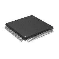
AD9882AKSTZ-100 Analog Devices Inc, AD9882AKSTZ-100 Datasheet - Page 17

AD9882AKSTZ-100
Manufacturer Part Number
AD9882AKSTZ-100
Description
IC INTERFACE/DVI 100MHZ 100LQFP
Manufacturer
Analog Devices Inc
Datasheet
1.AD9882KSTZ-100.pdf
(40 pages)
Specifications of AD9882AKSTZ-100
Applications
Video
Interface
Analog, DVI
Voltage - Supply
3.15 V ~ 3.45 V
Package / Case
100-LQFP
Mounting Type
Surface Mount
Supply Voltage Range
3.15V To 3.45V, 2.2V To 3.45V
Operating Temperature Range
0°C To +70°C
Digital Ic Case Style
LQFP
No. Of Pins
100
Msl
MSL 3 - 168 Hours
Update Rate
140MSPS
Bandwidth
300MHz
Rohs Compliant
Yes
Lead Free Status / RoHS Status
Lead free / RoHS Compliant
Available stocks
Company
Part Number
Manufacturer
Quantity
Price
Company:
Part Number:
AD9882AKSTZ-100
Manufacturer:
AD
Quantity:
1 200
Company:
Part Number:
AD9882AKSTZ-100
Manufacturer:
ADI
Quantity:
352
Company:
Part Number:
AD9882AKSTZ-100
Manufacturer:
Analog Devices Inc
Quantity:
10 000
Part Number:
AD9882AKSTZ-100
Manufacturer:
ADI/亚德诺
Quantity:
20 000
TIMING: ANALOG INTERFACE
The following timing diagrams show the operation of the
AD9882A. The output data clock signal is created so that its
rising edge always occurs between data transitions and can be
used to latch the output data externally.
Hsync Timing
Horizontal sync (Hsync) is processed in the AD9882A to
eliminate ambiguity in the timing of the leading edge with
respect to the phase-delayed pixel clock and data. The Hsync
input is used as a reference to generate the pixel sampling clock.
The sampling phase can be adjusted, with respect to Hsync,
through a full 360° in 32 steps via the phase adjust register
(Register 0x04) to optimize the pixel sampling time. Display
systems use Hsync to align memory and display write cycles, so
it is important to have a stable timing relationship between
Hsync output (HSOUT) and data clock (DATACK).
Three things happen to horizontal sync in the AD9882A. First,
the polarity of Hsync input is determined and therefore has a
known output polarity. The known output polarity can be
programmed either active high or active low (Register 0x10,
Bit 5). Second, HSOUT is aligned with DATACK and data
outputs. Third, the duration of HSOUT (in pixel clocks) is set
via Register 0x07. HSOUT is the sync signal that should be used
to drive the rest of the display system.
DATACK
HSOUT
DATA
t
t
DCYCLE
SKEW
Figure 9. Output Timing
t
SKEW
t
PER
Rev. 0 | Page 17 of 40
Coast Timing
In most computer systems, the Hsync signal is provided
continuously on a dedicated wire. In these systems, the
coast function is unnecessary and should be disabled using
Register 0x11, Bits 1 to 3.
In some systems, however, Hsync is disturbed during the verti-
cal sync period (Vsync). In other cases, Hsync pulses disappear.
In other systems, such as those that employ composite sync
(Csync) signals or embedded sync-on-green (SOG), Hsync
includes equalization pulses or other distortions during Vsync.
To avoid upsetting the clock generator during Vsync, it is
important to ignore these distortions. If the pixel clock PLL sees
extraneous pulses, it attempts to lock to this new frequency and
has changed frequency by the end of the Vsync period. It then
takes a few lines of correct Hsync timing to recover at the
beginning of a new frame, resulting in a tearing of the image at
the top of the display.
The coast function is provided to eliminate this problem. It is an
internally generated signal, created by the sync processing
engine that disables the PLL input and allows the clock to free-
run at its then-current frequency. The PLL can free-run for
several lines without significant frequency drift.
AD9882A


