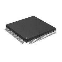
AD9882AKSTZ-100 Analog Devices Inc, AD9882AKSTZ-100 Datasheet - Page 27

AD9882AKSTZ-100
Manufacturer Part Number
AD9882AKSTZ-100
Description
IC INTERFACE/DVI 100MHZ 100LQFP
Manufacturer
Analog Devices Inc
Datasheet
1.AD9882KSTZ-100.pdf
(40 pages)
Specifications of AD9882AKSTZ-100
Applications
Video
Interface
Analog, DVI
Voltage - Supply
3.15 V ~ 3.45 V
Package / Case
100-LQFP
Mounting Type
Surface Mount
Supply Voltage Range
3.15V To 3.45V, 2.2V To 3.45V
Operating Temperature Range
0°C To +70°C
Digital Ic Case Style
LQFP
No. Of Pins
100
Msl
MSL 3 - 168 Hours
Update Rate
140MSPS
Bandwidth
300MHz
Rohs Compliant
Yes
Lead Free Status / RoHS Status
Lead free / RoHS Compliant
Available stocks
Company
Part Number
Manufacturer
Quantity
Price
Company:
Part Number:
AD9882AKSTZ-100
Manufacturer:
AD
Quantity:
1 200
Company:
Part Number:
AD9882AKSTZ-100
Manufacturer:
ADI
Quantity:
352
Company:
Part Number:
AD9882AKSTZ-100
Manufacturer:
Analog Devices Inc
Quantity:
10 000
Part Number:
AD9882AKSTZ-100
Manufacturer:
ADI/亚德诺
Quantity:
20 000
CLAMP TIMING
0x05 7–0
An 8-bit register that sets the position of the internally
generated clamp.
When clamp function (Register 0x11, Bit 7) is 0, a clamp signal
is generated internally at a position established by the clamp
placement and for a duration set by the clamp duration.
Clamping is started (clamp placement) an integral number of
pixel periods after the trailing edge of Hsync. The clamp
placement can be programmed to any value from 1 to 255.
The clamp should be placed during a time that the input signal
presents a stable black-level reference, usually the back porch
period between Hsync and the image.
When clamp function is 1, this register is ignored.
0x06 7–0
An 8-bit register that sets the duration of the internally
generated clamp.
For the best results, the clamp duration should be set to include
the majority of the black-reference signal time that follows the
Hsync signal trailing edge. Insufficient clamping time can pro-
duce brightness changes at the top of the screen and a slow
recovery from large changes in the average picture level (APL)
or brightness.
When clamp function is 1, this register is ignored.
HSYNC OUTPUT PULSE WIDTH
0x07 7–0
An 8-bit register that sets the duration of the Hsync output
pulse.
The leading edge of the Hsync output is triggered by the
internally generated, phase-adjusted PLL feedback clock. The
AD9882A then counts a number of pixel clocks equal to the
value in this register minus one. This triggers the trailing edge
of the Hsync output, which is also phase-adjusted.
INPUT GAIN
0x08 7–0
An 8-bit word that sets the gain of the red channel. The
AD9882A can accommodate input signals with a full-scale
range of between 0.5 V and 1.0 V p-p. Setting red gain to 255
corresponds to an input range of 1.0 V. A red gain of 0
establishes an input range of 0.5 V. Note that increasing red gain
results in the picture having less contrast (the input signal uses
fewer of the available converter codes). See Figure 4.
0x09 7–0
An 8-bit word that sets the gain of the green channel. See red
gain (0x08).
Clamp Placement
Clamp Duration
Hsync Output Pulse Width
Red Gain
Green Gain
Red Gain
Green Gain
Rev. 0 | Page 27 of 40
0x0A 7–0
An 8-bit word that sets the gain of the blue channel. See Red
gain (0x08).
INPUT OFFSET
0x0B 7–1
A 7-bit offset binary word that sets the dc offset of the red chan-
nel. One LSB of offset adjustment equals approximately one LSB
change in the ADC offset. Therefore, the absolute magnitude of
the offset adjustment scales as the gain of the channel changes.
A nominal setting of 64 results in the channel nominally clamp-
ing the back porch (during the clamping interval) to Code 00.
An offset setting of 127 results in the channel clamping to
Code 63 of the ADC. An offset setting of 0 clamps to Code –64
(off the bottom of the range). Increasing the value of the red
offset decreases the brightness of the channel.
0x0C 7–1
A 7-bit offset binary word that sets the dc offset of the green
channel. See the 0x0B 7–1 red channel offset adjust.
0x0D 7–1
A 7-bit offset binary word that sets the dc offset of the blue
channel. 0x0B 7–1 Red channel offset adjust.
0x0E 7–0
This register is used to set the responsiveness of the sync
separator. It sets how many internal 5 MHz clock periods the
sync separator must count to before toggling high or low. It
works like a low-pass filter to ignore Hsync pulses in order to
extract the Vsync signal. This register should be set to some
number greater than the maximum Hsync pulse width. Note
that the sync separator threshold uses an internal dedicated
clock with a frequency of approximately 5 MHz.
The default for this register is 0x20.
0x0F 7–3
This register allows the comparator threshold of the sync-on-
green slicer to be adjusted. This register adjusts it in steps of
10 mV, with the minimum setting equaling 10 mV and the
maximum setting equaling 330 mV.
The default setting is 15 decimal and corresponds to a threshold
value of 170 mV.
0x0F 2
This bit is used to override the automatic interface selection
(Bit 3 in Register 0x15). To override, set this bit to Logic 1.
When overriding, the active interface is set via Bit 1 in this
register.
Table 15. Active Interface Override Settings
AIO
0
1
The default for this register is 0.
Result
Autodetermines the active interface.
Override; Bit 1 determines the active interface.
AIO Active Interface Override
Blue Gain
Red Channel Offset Adjust
Green Channel Offset Adjust
Blue Channel Offset Adjust
Sync Separator Threshold
Sync-on-Green Slicer Threshold
Blue Gain
AD9882A


