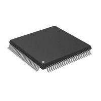
AD9882AKSTZ-100 Analog Devices Inc, AD9882AKSTZ-100 Datasheet - Page 14

AD9882AKSTZ-100
Manufacturer Part Number
AD9882AKSTZ-100
Description
IC INTERFACE/DVI 100MHZ 100LQFP
Manufacturer
Analog Devices Inc
Datasheet
1.AD9882KSTZ-100.pdf
(40 pages)
Specifications of AD9882AKSTZ-100
Applications
Video
Interface
Analog, DVI
Voltage - Supply
3.15 V ~ 3.45 V
Package / Case
100-LQFP
Mounting Type
Surface Mount
Supply Voltage Range
3.15V To 3.45V, 2.2V To 3.45V
Operating Temperature Range
0°C To +70°C
Digital Ic Case Style
LQFP
No. Of Pins
100
Msl
MSL 3 - 168 Hours
Update Rate
140MSPS
Bandwidth
300MHz
Rohs Compliant
Yes
Lead Free Status / RoHS Status
Lead free / RoHS Compliant
Available stocks
Company
Part Number
Manufacturer
Quantity
Price
Company:
Part Number:
AD9882AKSTZ-100
Manufacturer:
AD
Quantity:
1 200
Company:
Part Number:
AD9882AKSTZ-100
Manufacturer:
ADI
Quantity:
352
Company:
Part Number:
AD9882AKSTZ-100
Manufacturer:
Analog Devices Inc
Quantity:
10 000
Part Number:
AD9882AKSTZ-100
Manufacturer:
ADI/亚德诺
Quantity:
20 000
AD9882A
An offset is then introduced, which results in the ADC
producing a black output (Code 0x00) when the known black
input is present. The offset then remains in place when other
signal levels are processed, and the entire signal is shifted to
eliminate offset errors.
In systems with embedded sync, a blacker-than-black signal
(Hsync) is produced briefly to signal the CRT that it is time to
begin a retrace. For obvious reasons, it is important to avoid
clamping on the tip of Hsync. Fortunately, there is virtually
always a period following Hsync called the back porch, in which
a good black reference is provided. This is the time when
clamping should be done.
The clamp timing is established by the AD9882A internal clamp
timing generator. The clamp placement register (0x05) is
programmed with the number of pixel times that should pass
after the trailing edge of Hsync before clamping starts. A second
register (clamp duration, 0x06) sets the duration of the clamp.
These are both 8-bit values, providing considerable flexibility in
clamp generation. The clamp timing is referenced to the trailing
edge of Hsync, because the back porch (black reference) always
follows Hsync. A good starting point for establishing clamping
is to set the clamp placement to 0x08 (providing eight pixel
periods for the graphics signal to stabilize after sync) and set the
clamp duration to 0x14 (giving the clamp 20 pixel periods to
reestablish the black reference).
The value of the external input coupling capacitor affects the
performance of the clamp. If the value is too small, there can be
an amplitude change during a horizontal line time (between
clamping intervals). If the capacitor is too large, then it takes
excessively long for the clamp to recover from a large change in
incoming signal offset. The recommended value (47 nF) results
in recovery from a step error of 100 mV to within one-half LSB
in 30 lines, using a clamp duration of 20 pixel periods on a
75 Hz SXGA signal.
YUV Clamping
YUV signals are slightly different from RGB signals in that the
dc reference level (black level in RGB signals) is at the midpoint
of the U and V video. For these signals, it might be necessary to
clamp to the midscale range of the ADC range (0x80) rather
than the bottom of the ADC range (0x00).
Clamping to midscale rather than ground can be accomplished
by setting the clamp select bits in the serial bus register. Each of
the three converters has its own selection bit, so that they can be
clamped to either midscale or ground independently. These bits
are located in Register 0x11 and are Bits 4 to 6. The midscale
reference voltage that each ADC clamps to is provided on the
MIDBYPASS pin (Pin 74). This pin should be bypassed to
ground with a 0.1 µF capacitor (even if midscale clamping is not
required).
Rev. 0 | Page 14 of 40
GAIN AND OFFSET CONTROL
The AD9882A can accommodate input signals with inputs
ranging from 0.5 V to 1.0 V full scale. The full-scale range is set
in three 8-bit registers (red gain, green gain, and blue gain).
A code of 0 establishes a minimum input range of 0.5 V; a code
of 255 corresponds with the maximum range of 1.0 V. Note that
increasing the gain setting results in an image with less contrast.
The offset control shifts the entire input range, resulting in a
change in image brightness. Three 7-bit registers (red offset,
green offset, and blue offset) provide independent settings for
each channel.
The offset controls provide a ±63 LSB adjustment range. This
range is connected with the full-scale range, so if the input
range is doubled (from 0.5 V to 1.0 V), the offset step size is also
doubled (from 2 mV per step to 4 mV per step).
Figure 4 illustrates the interaction of gain and offset controls.
The magnitude of an LSB in offset adjustment is proportional to
the full-scale range, so changing the full-scale range also
changes the offset. The change is minimal if the offset setting is
near midscale. When changing the offset, the full-scale range is
not affected, but the full-scale level is shifted by the same
amount as the zero-scale level.
1.0 V
0.5 V
0.0 V
0x00
Figure 4. Gain and Offset Control
OFFSET = 0x3F
GAIN
0xFF


