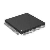
AD9882AKSTZ-100 Analog Devices Inc, AD9882AKSTZ-100 Datasheet - Page 33

AD9882AKSTZ-100
Manufacturer Part Number
AD9882AKSTZ-100
Description
IC INTERFACE/DVI 100MHZ 100LQFP
Manufacturer
Analog Devices Inc
Datasheet
1.AD9882KSTZ-100.pdf
(40 pages)
Specifications of AD9882AKSTZ-100
Applications
Video
Interface
Analog, DVI
Voltage - Supply
3.15 V ~ 3.45 V
Package / Case
100-LQFP
Mounting Type
Surface Mount
Supply Voltage Range
3.15V To 3.45V, 2.2V To 3.45V
Operating Temperature Range
0°C To +70°C
Digital Ic Case Style
LQFP
No. Of Pins
100
Msl
MSL 3 - 168 Hours
Update Rate
140MSPS
Bandwidth
300MHz
Rohs Compliant
Yes
Lead Free Status / RoHS Status
Lead free / RoHS Compliant
Available stocks
Company
Part Number
Manufacturer
Quantity
Price
Company:
Part Number:
AD9882AKSTZ-100
Manufacturer:
AD
Quantity:
1 200
Company:
Part Number:
AD9882AKSTZ-100
Manufacturer:
ADI
Quantity:
352
Company:
Part Number:
AD9882AKSTZ-100
Manufacturer:
Analog Devices Inc
Quantity:
10 000
Part Number:
AD9882AKSTZ-100
Manufacturer:
ADI/亚德诺
Quantity:
20 000
change only when SCL is low. If SDA changes state while SCL is
high, the serial interface interprets that action as a start or stop
sequence.
The five components to serial bus operation are
•
•
•
•
•
When the serial interface is inactive (SCL and SDA are high),
communications are initiated by sending a start signal. The start
signal is a high-to-low transition on SDA while SCL is high.
This signal alerts all slaved devices that a data transfer sequence
is coming.
The first eight bits of data transferred after a start signal com-
prise a 7-bit slave address (the first seven bits) and a single R/ W
bit (the eighth bit). The R/ W bit indicates the direction of data
transfer: read from (1) or write to (0) the slave device. If the
transmitted slave address matches the address of the device
(set by the state of the SA input pin listed in Table 52), the
AD9882A acknowledges by bringing SDA low on the ninth
SCL pulse. If the addresses do not match, the AD9882A does
not acknowledge.
Table 52. Serial Port Addresses
Bit 7
A6
(MSB)
1
1
Data Transfer via Serial Interface
For each byte of data read or written, the MSB is the first bit of
the sequence. If the AD9882A does not acknowledge the master
device during a write sequence, the SDA remains high so the
master can gen-erate a stop signal. If the master device does not
Start signal
Slave address byte
Base register address byte
Data byte to read or write
Stop signal
Bit 6
A5
0
0
SDA
SCL
Bit 5
A4
0
0
t
STAH
t
BUFF
Bit 4
A3
1
1
t
SDA
SCL
DHO
Bit 3
A2
1
1
BIT 7
Bit 2
A1
0
0
t
DAL
Figure 19. Serial Interface, Typical Byte Transfer
BIT 6
Figure 18. Serial Port Read/Write Timing
t
DAH
BIT 5 BIT 4 BIT 3 BIT 2 BIT 1
Bit 1
A0
(LSB)
0
1
t
DSU
Rev. 0 | Page 33 of 40
acknowledge the AD9882A during a read sequence, the
AD9882A interprets this as end of data. The SDA remains
high so the master can generate a stop signal.
Writing data to specific control registers of the AD9882A
requires that the 8-bit address of the control register of interest
be written after the slave address has been established. This
control register address is the base address for subsequent write
operations. The base address autoincrements by one for each
byte of data written after the data byte intended for the base
address. If there are more bytes transferred than there are avail-
able addresses, the address does not increment and remains at
its maximum value of 0x1E. Any base address higher than 0x1E
does not produce an acknowledge signal.
Data is read from the control registers of the AD9882A in a
similar manner. Reading requires two data transfer operations:
•
•
To terminate a read/write sequence to the AD9882A, a stop
signal must be sent. A stop signal comprises a low-to-high
transition of SDA while SCL is high. The timing for the
read/write is shown in Figure 18, and a typical byte transfer is
shown in Figure 19.
A repeated start signal occurs when the master device driving
the serial interface generates a start signal without first gener-
ating a stop signal to terminate the current communication.
This is used to change the mode of communication (read, write)
between the slave and master without releasing the serial
interface lines.
The base address must be written with the R/ W bit of the
slave address byte low to set up a sequential read operation.
Reading (the R/ W bit of the slave address byte high) begins
at the previously established base address. The address of
the read register autoincrements after each byte is
transferred.
t
STASU
BIT 0
ACK
t
STOSU
AD9882A


