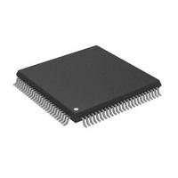
AD9882AKSTZ-100 Analog Devices Inc, AD9882AKSTZ-100 Datasheet - Page 24

AD9882AKSTZ-100
Manufacturer Part Number
AD9882AKSTZ-100
Description
IC INTERFACE/DVI 100MHZ 100LQFP
Manufacturer
Analog Devices Inc
Datasheet
1.AD9882KSTZ-100.pdf
(40 pages)
Specifications of AD9882AKSTZ-100
Applications
Video
Interface
Analog, DVI
Voltage - Supply
3.15 V ~ 3.45 V
Package / Case
100-LQFP
Mounting Type
Surface Mount
Supply Voltage Range
3.15V To 3.45V, 2.2V To 3.45V
Operating Temperature Range
0°C To +70°C
Digital Ic Case Style
LQFP
No. Of Pins
100
Msl
MSL 3 - 168 Hours
Update Rate
140MSPS
Bandwidth
300MHz
Rohs Compliant
Yes
Lead Free Status / RoHS Status
Lead free / RoHS Compliant
Available stocks
Company
Part Number
Manufacturer
Quantity
Price
Company:
Part Number:
AD9882AKSTZ-100
Manufacturer:
AD
Quantity:
1 200
Company:
Part Number:
AD9882AKSTZ-100
Manufacturer:
ADI
Quantity:
352
Company:
Part Number:
AD9882AKSTZ-100
Manufacturer:
Analog Devices Inc
Quantity:
10 000
Part Number:
AD9882AKSTZ-100
Manufacturer:
ADI/亚德诺
Quantity:
20 000
AD9882A
Hexadecimal
Address
0x11
0x12
0x13
0x14
0x15
Read and
Write or
Read Only
R/W
R/W
R/W
R/W
RO
Bit
4
3
2
1
0
7
6
5
4
3
2
1
7–0
7–0
7–6
5
4
3
2
1
0
7
6
5
4
3
Default
Value
***0 ****
**** 0***
**** *0**
**** **0*
**** ***0
0*** ****
*0** ****
**0* ****
***0 ****
**** 1***
**** *0**
**** **1*
0000 0000
0000 0000
11** ****
**1* ****
***0 ****
**** 0***
**** *0**
**** **1*
**** ***0
Register Name
Active Hsync
Override
Active Hsync
Select
Output Vsync
Polarity
Active Vsync
Override
Active Vsync
Select
Clamp Function
Red Clamp Select
Green Clamp
Select
Blue Clamp Select
Coast Select
Coast Polarity
Override
Input Coast
Polarity
Precoast
Postcoast
Output Drive
Select
Programmable
Bandwidth
DVI Clock Invert
DVI PDO Three-
State
HDCP Address
Power-Down
Enable 4:2:2
Analog Hsync
Active
Analog SOG
Active
Analog Vsync
Active
DVI Active
Active Interface
Rev. 0 | Page 24 of 40
0 = No override.
1 = User overrides, analog Hsync set by 0x10, Bit 3.
0 = Analog Hsync from the Hsync input pin.
1 = Analog Hsync from SOG. This bit is used if Register 0x10, Bit 4
is set to 1 or if both syncs are active.
0 = Invert.
1 = Not inverted.
0 = No override.
1 = User overrides, analog Vsync set by 0x10, Bit 0.
0 = Analog Vsync from the Vsync input pin.
1 = Analog Vsync from sync separator.
0 = Clamping with internal clamp.
1 = Clamping disabled.
0 = Clamp to ground.
1 = Clamp to midscale for red channel.
0 = Clamp to ground.
1 = Clamp to midscale for green channel.
0 = Clamp to ground.
1 = Clamp to midscale for blue channel.
0 = Disabled coast.
1 = Coasting with internally generated coast signal.
0 = Coast polarity determined by the chip.
1 = Coast polarity set by 0x11, Bit 1. This bit must be set to 1 to
disable coast.
0 = Active low coast signal.
1 = Active high coast signal. This bit must be set to 1 to disable
coast.
Number of Hsync periods that coast goes active prior to Vsync.
Number of Hsync periods before coast goes inactive following
Vsync.
Selects among high, medium, and low output drive strength.
0 = Low bandwidth of 10 MHz.
1 = High bandwidth of 300 MHz.
0 = DVI data clock output not inverted.
1 = DVI data clock output inverted.
For digital interface only.
0 = Normal outputs.
1 = High impedance outputs.
Address Bit 1 = 1 for HDCP slave port.
0 = Full chip power-down.
0 = 4:4:4 mode.
1 = 4:2:2 mode.
0 = Hsync not detected.
1 = Hsync detected.
0 = Sync signal not detected on green channel.
1 = Sync signal detected on green channel.
0 = Vsync not detected.
1 = Vsync detected.
0 = Digital interface clock not detected.
1 = Digital interface clock detected.
0 = Analog interface active.
1 = DVI interface active.
Function
Address Bit 0 = 0 for HDCP slave port.


