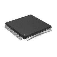
AD9882AKSTZ-100 Analog Devices Inc, AD9882AKSTZ-100 Datasheet - Page 37

AD9882AKSTZ-100
Manufacturer Part Number
AD9882AKSTZ-100
Description
IC INTERFACE/DVI 100MHZ 100LQFP
Manufacturer
Analog Devices Inc
Datasheet
1.AD9882KSTZ-100.pdf
(40 pages)
Specifications of AD9882AKSTZ-100
Applications
Video
Interface
Analog, DVI
Voltage - Supply
3.15 V ~ 3.45 V
Package / Case
100-LQFP
Mounting Type
Surface Mount
Supply Voltage Range
3.15V To 3.45V, 2.2V To 3.45V
Operating Temperature Range
0°C To +70°C
Digital Ic Case Style
LQFP
No. Of Pins
100
Msl
MSL 3 - 168 Hours
Update Rate
140MSPS
Bandwidth
300MHz
Rohs Compliant
Yes
Lead Free Status / RoHS Status
Lead free / RoHS Compliant
Available stocks
Company
Part Number
Manufacturer
Quantity
Price
Company:
Part Number:
AD9882AKSTZ-100
Manufacturer:
AD
Quantity:
1 200
Company:
Part Number:
AD9882AKSTZ-100
Manufacturer:
ADI
Quantity:
352
Company:
Part Number:
AD9882AKSTZ-100
Manufacturer:
Analog Devices Inc
Quantity:
10 000
Part Number:
AD9882AKSTZ-100
Manufacturer:
ADI/亚德诺
Quantity:
20 000
PLL
Place the PLL loop filter components as close to the FILT pin as
possible.
Do not place any digital or other high frequency traces near
these components.
Use the values suggested in the data sheet with 10% or smaller
tolerances.
OUTPUTS: DATA AND CLOCKS
Try to minimize the trace length that the digital outputs have to
drive. Longer traces have higher capacitance and require more
current, which causes more internal digital noise.
Shorter traces reduce the possibility of reflections.
Adding a series resistor with a value of 22 Ω to 100 Ω can
suppress reflections, reduce EMI, and reduce the current spikes
inside of the AD9882A. However, if 50 Ω traces are used on the
PCB, the data output should not need these resistors.
A 22 Ω resistor on the DATACK output should provide good
impedance matching that can reduce reflections. If EMI or
current spiking is a concern, use a lower drive strength setting
Rev. 0 | Page 37 of 40
by adjusting Register 0x14. If series resistors are used, place
them as close as possible to the AD9882A pins but avoid adding
vias or extra length to the output trace to get the resistors closer.
If possible, limit the capacitance that each of the digital outputs
drives to less than 10 pF by keeping traces short and connecting
the outputs to only one device. Loading the outputs with
excessive capacitance increases the current transients inside the
AD9882A, creating more digital noise on its power supplies.
DIGITAL INPUTS
The digital inputs on the AD9882A were designed to work with
3.3 V signals, but are tolerant of 5.0 V signals. No extra
components need to be added, if 5.0 V logic is used.
Any noise that gets onto the Hsync input trace adds jitter to the
system. Therefore, minimize the trace length and do not run
any digital or other high frequency traces near it.
VOLTAGE REFERENCE
Bypass with a 0.1 µF capacitor. Place as close as possible to the
AD9882A pin. Make the ground connection as short as
possible.
AD9882A


