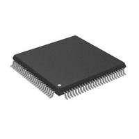
AD9882AKSTZ-100 Analog Devices Inc, AD9882AKSTZ-100 Datasheet - Page 12

AD9882AKSTZ-100
Manufacturer Part Number
AD9882AKSTZ-100
Description
IC INTERFACE/DVI 100MHZ 100LQFP
Manufacturer
Analog Devices Inc
Datasheet
1.AD9882KSTZ-100.pdf
(40 pages)
Specifications of AD9882AKSTZ-100
Applications
Video
Interface
Analog, DVI
Voltage - Supply
3.15 V ~ 3.45 V
Package / Case
100-LQFP
Mounting Type
Surface Mount
Supply Voltage Range
3.15V To 3.45V, 2.2V To 3.45V
Operating Temperature Range
0°C To +70°C
Digital Ic Case Style
LQFP
No. Of Pins
100
Msl
MSL 3 - 168 Hours
Update Rate
140MSPS
Bandwidth
300MHz
Rohs Compliant
Yes
Lead Free Status / RoHS Status
Lead free / RoHS Compliant
Available stocks
Company
Part Number
Manufacturer
Quantity
Price
Company:
Part Number:
AD9882AKSTZ-100
Manufacturer:
AD
Quantity:
1 200
Company:
Part Number:
AD9882AKSTZ-100
Manufacturer:
ADI
Quantity:
352
Company:
Part Number:
AD9882AKSTZ-100
Manufacturer:
Analog Devices Inc
Quantity:
10 000
Part Number:
AD9882AKSTZ-100
Manufacturer:
ADI/亚德诺
Quantity:
20 000
AD9882A
THEORY OF OPERATION: INTERFACE DETECTION
ACTIVE INTERFACE DETECTION AND SELECTION
The AD9882A includes circuitry to detect whether an interface
is active or not (see Table 6).
For detecting the analog interface, the circuitry monitors the
presence of Hsync, Vsync, and sync-on-green. The result of the
detection circuitry can be read from the 2-wire serial interface
bus at Address 0x15, Bits 7, 5, and 6, respectively. If one of these
sync signals disappears, the maximum time it takes for the
circuitry to detect it is 100 ms.
For detecting the digital interface, there are two stages of
detection. The first stage searches for the presence of the digital
interface clock. The circuitry for detecting the digital interface
clock is active even when the digital interface is powered down.
The result of this detection stage can be read from the 2-wire
serial interface bus at Address 0x15, Bit 4. If the clock disap-
pears, the maximum time it takes for the circuitry to detect it is
100 ms. Once a digital interface clock is detected, the digital
interface is powered up and the second stage of detection
begins. During the second stage, the circuitry searches for
32 consecutive DEs. Once 32 DEs are found, the detection
process is complete.
There is an override for the automatic interface selection. It is
the AIO (Active Interface Override) bit, Register 0x0F, Bit 2.
When the AIO bit is set to Logic 0, the automatic circuitry is
used. When the AIO bit is set to Logic 1, the AIS (Active
Interface Select) bit (Register 0x0F, Bit 1) is used to determine
the active interface rather than the automatic circuitry.
Rev. 0 | Page 12 of 40
POWER MANAGEMENT
The AD9882A is a dual interface device with shared outputs.
Only one interface can be used at a time. For this reason, the
chip automatically powers down the unused interface. When
the analog interface is being used, most of the digital interface
circuitry is powered down, and vice versa. This helps to mini-
mize the AD9882A total power dissipation. In addition, if
neither interface has activity on it, the chip powers down both
interfaces. The AD9882A uses the activity detect circuits, the
active interface bits in Serial Register 0x15, the active interface
override bits in Register 0x0F, Bits 2 and 1, and the power-down
bit in Register 0x14, Bit 1, to determine the correct power state.
In a given power mode, not all circuitry in the inactive interface
is powered down completely.
When the digital interface is active, the band gap reference
Hsync, Vsync, and SOG detect circuitry remain powered-up.
When the analog interface is active, the digital interface clock
detect circuit is not powered-down. Table 7 summarizes how
the AD9882A determines which power mode to be in and
which circuitry is powered on/off in each of these modes. The
power-down command has priority, then the active interface
override, and then the automatic circuitry.


